
herunterladen
Semiconductor Components Industries, LLC, 2012
February, 2012 − Rev. 9
1 Publication Order Number:
MJD6039/D
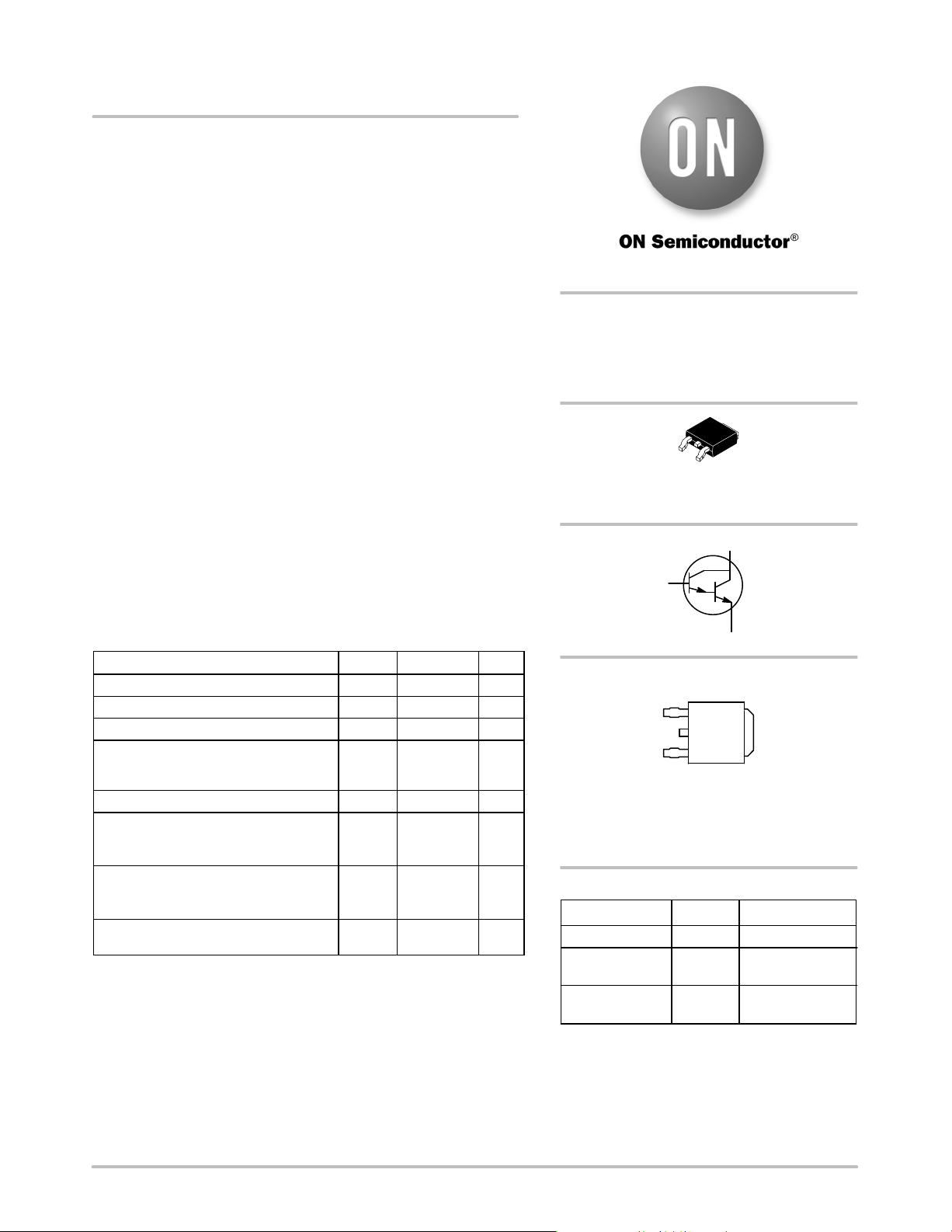
MJD6039, NJVMJD6039T4G
Darlington Power
Transistors
DPAK For Surface Mount Applications
Designed for general purpose power and switching such as output or
driver stages in applications such as switching regulators, convertors,
and power amplifiers.
Features
Lead Formed for Surface Mount Applications in Plastic Sleeves
(No Suffix)
Straight Lead Version in Plastic Sleeves (“−1” Suffix)
Monolithic Construction With Built−in Base−Emitter Shunt Resistors
High DC Current Gain − h
FE
= 2500 (Typ) @ I
C
= 4.0 Adc
Epoxy Meets UL 94 V−0 @ 0.125 in
ESD Ratings:
Human Body Model, 3B > 8000 V
Machine Model, C > 400 V
NJV Prefix for Automotive and Other Applications Requiring
Unique Site and Control Change Requirements; AEC−Q101
Qualified and PPAP Capable
Pb−Free Package is Available*
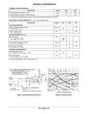
MAXIMUM RATINGS
Rating Symbol Max Unit
Collector−Emitter Voltage V
CEO
80 Vdc
Collector−Base Voltage V
CB
80 Vdc
Emitter−Base Voltage V
EB
5 Vdc
Collector Current
Continuous
Peak
I
C
4
8
Adc
Base Current I
B
100 mAdc
Total Power Dissipation
@ T
C
= 25C
Derate above 25C
P
D
20
0.16
W
W/C
Total Power Dissipation (Note 1)
@ T
A
= 25C
Derate above 25C
P
D
1.75
0.014
W
W/C
Operating and Storage Junction
Temperature Range
T
J
, T
stg
−65 to +150 C
Stresses exceeding Maximum Ratings may damage the device. Maximum
Ratings are stress ratings only. Functional operation above the Recommended
Operating Conditions is not implied. Extended exposure to stresses above the
Recommended Operating Conditions may affect device reliability.
1. These ratings are applicable when surface mounted on the minimum pad
sizes recommended.
*For additional information on our Pb−Free strategy and soldering details, please
download the ON Semiconductor Soldering and Mounting Techniques
Reference Manual, SOLDERRM/D.
SILICON
POWER TRANSISTORS
4 AMPERES,
80 VOLTS, 20 WATTS
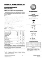
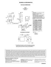
MARKING DIAGRAM
A = Assembly Location
Y = Year
WW = Work Week
J6039 = Device Code
G = Pb−Free Package
DPAK
CASE 369C
STYLE 1
AYWW
J
6039G
Device Package Shipping
†
ORDERING INFORMATION
MJD6039T4 DPAK 2,500/Tape & Reel
†For information on tape and reel specifications,
including part orientation and tape sizes, please
refer to our Tape and Reel Packaging Specifications
Brochure, BRD8011/D.
http://onsemi.com
MJD6039T4G DPAK
(Pb−Free)
2,500/Tape & Reel
COLLECTOR 2, 4
BASE
1
EMITTER 3
NJVMJD6039T4G DPAK
(Pb−Free)
2,500/Tape & Reel
Verzeichnis
- ・ Abmessungen des Paketumrisses on Seite 5
- ・ Paket-Footprint-Pad-Layout on Seite 5
- ・ Teilenummerierungssystem on Seite 1 Seite 5
- ・ Markierungsinformationen on Seite 1
- ・ Blockdiagramm on Seite 4
- ・ Technische Daten on Seite 1
- ・ Anwendungsbereich on Seite 1
- ・ Elektrische Spezifikation on Seite 2 Seite 3 Seite 4