
herunterladen
© 2006 Microchip Technology Inc. DS01030A-page 1
AN1030
INTRODUCTION
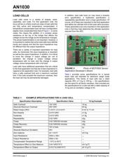
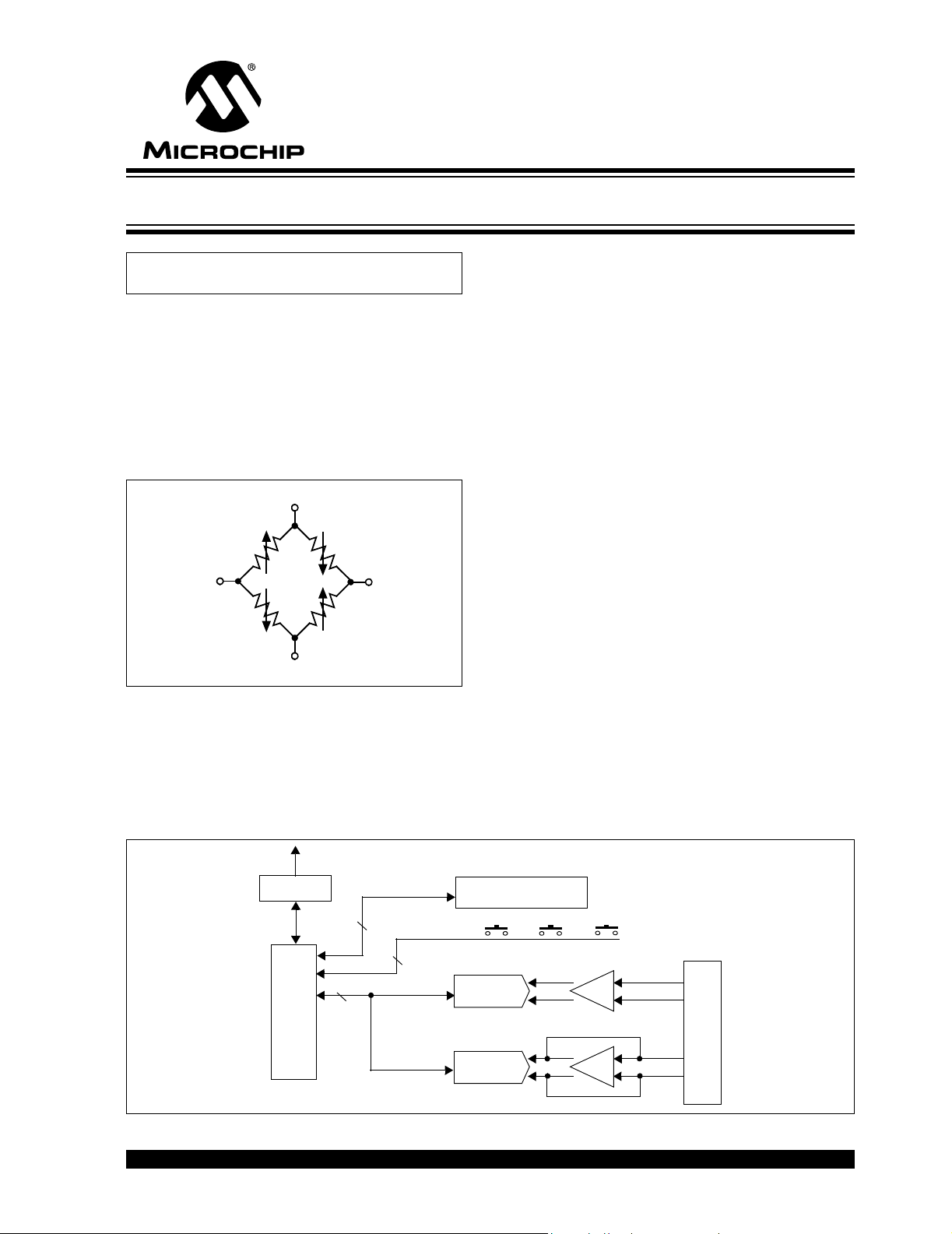
There are many different types of sensors whose
underlying realization is based on a Wheatstone
bridge. Strain gauges are one such sensor. As a
material is strained, there is a corresponding change in
resistance. In many cases, each side of the Wheat-
stone bridge may respond to the strain by lowering or
increasing in resistance (see Figure 1).
FIGURE 1: Wheatstone Bridge of a
Typical Strain Gauge.
In the case of Figure 1, the bridge is said to be fully
active. In some cases, only half of the bridge may be
active (half active). For some sensors, only a single
element of the bridge may change in response to the
stimulus.
This application note will focus specifically on load
cells, a type of strain gauge that is typically used for
measuring weight. Even more specifically, the focus
will be on fully active, temperature compensated load
cells whose change in differential output voltage with a
rated load is 2 mV to 4 mV per volt of excitation (the
excitation voltage being the difference between the
+Input and the –Input terminals of the load cell).
The goal is to develop a variety of circuits that can
quantify this change via an analog-to-digital converter
(ADC), which will be a MCP3551, 22-bit Delta-Sigma
ADC. The analysis for each circuit should be applicable
to other resistive bridge sensors. The different circuits
will allow cost versus performance trade-offs.
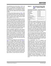
The circuits presented in this application note have
been realized in the MCP355X Sensor Application
Developer’s Board whose block diagram is shown in
Figure 2. This board includes two microcontrollers. The
PIC16F877 performs the basic weigh scale function
while the PIC18F4550 sends data to a personal com-
puter (PC) for analysis and debugging. The board
includes a display as well as input switches that are
used for calibrating the zero point and full-scale point of
the load cell and for setting various processing options.
Conversion results from the currently selected ADC are
communicated to the PC over the USB bus. This data
can be viewed on a PC using the DataView software
that comes with the reference design. All of the testing
and results shown in this application note were done
with an MCP355X Sensor Application Developer’s
Board, the DataView software, and various load cells
and/or load cell simulators that are either described in
this document or that can be easily purchased.
FIGURE 2: MCP355X Sensor Application Developer’s Board Functional Block Diagram.
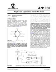
Author: Jerry Horn, Gordon Gleason
Lynium, L.L.C.
+Output –Output
Tension Compression
Compression Tension
–Input
+Input
Push Button Control Switches
PIC18F4550
PIC16F877
SPI
LCD Display
I
2
C
GAIN
Channel 1
USB to PC running DataView
MCP3551 ΔΣ
ADC
GAIN
Channel 2
Sensor Input Connections
8
3
4
MCP3551 ΔΣ
ADC
Weigh Scale Applications for the MCP3551
Verzeichnis
- ・ Blockdiagramm on Seite 1 Seite 10
- ・ Technische Daten on Seite 2 Seite 3 Seite 5
- ・ Anwendungsbereich on Seite 1