

herunterladen
NXP Semiconductors
Data Sheet: Technical Data
Document Number: IMX6ULLIEC
Rev. 1.1, 05/2017
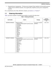
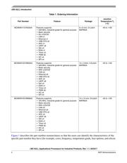
Ordering Information
See Table 1 on page 3
MCIMX6Y0CVM05AA MCIMX6Y1CVM05AA
MCIMX6Y1CVK05AA MCIMX6Y2CVM05AA
MCIMX6Y2CVM08AA
Package Information
Plastic Package
MAPBGA 14 x 14 mm, 0.8 mm pitch
MAPBGA 9 x 9 mm, 0.5 mm pitch
© 2016-2017 NXP B.V.
1 i.MX 6ULL Introduction
The i.MX 6ULL processors represent NXP’s latest
achievement in integrated multimedia-focused products
offering high performance processing with a high degree
of functional integration, targeted towards the growing
market of connected devices.
The i.MX 6ULL is a high performance, ultra efficient
processor family with featuring NXP’s advanced
implementation of the single ARM Cortex
®
-A7 core,
which operates at speeds of up to 792 MHz. i.MX 6ULL
includes integrated power management module that
reduces the complexity of external power supply and
simplifies the power sequencing. Each processor in this
family provides various memory interfaces, including
LPDDR2, DDR3, DDR3L, Raw and Managed NAND
flash, NOR flash, eMMC, Quad SPI, and a wide range of
other interfaces for connecting peripherals, such as
WLAN, Bluetooth™, GPS, displays, and camera
sensors.
i.MX 6ULL Applications
Processors for Industrial
Products
1. i.MX 6ULL Introduction . . . . . . . . . . . . . . . . . . . . . . . . . . 1
1.1. Ordering Information . . . . . . . . . . . . . . . . . . . . . . . 3
1.2. Features . . . . . . . . . . . . . . . . . . . . . . . . . . . . . . . . . 5
2. Architectural Overview . . . . . . . . . . . . . . . . . . . . . . . . . . . 9
2.1. Block Diagram . . . . . . . . . . . . . . . . . . . . . . . . . . . . 9
3. Modules List . . . . . . . . . . . . . . . . . . . . . . . . . . . . . . . . . . 10
3.1. Special Signal Considerations . . . . . . . . . . . . . . . 17
3.2. Recommended Connections for Unused Analog
Interfaces . . . . . . . . . . . . . . . . . . . . . . . . . . . . . . . 18
4. Electrical Characteristics . . . . . . . . . . . . . . . . . . . . . . . . 20
4.1. Chip-Level Conditions . . . . . . . . . . . . . . . . . . . . . 20
4.2. Power Supplies Requirements and Restrictions . 30
4.3. Integrated LDO Voltage Regulator Parameters . . 31
4.4. PLL’s Electrical Characteristics . . . . . . . . . . . . . . . 33
4.5. On-Chip Oscillators . . . . . . . . . . . . . . . . . . . . . . . 35
4.6. I/O DC Parameters . . . . . . . . . . . . . . . . . . . . . . . . 36
4.7. I/O AC Parameters . . . . . . . . . . . . . . . . . . . . . . . . 39
4.8. Output Buffer Impedance Parameters . . . . . . . . . 42
4.9. System Modules Timing . . . . . . . . . . . . . . . . . . . . 45
4.10. Multi-Mode DDR Controller (MMDC) . . . . . . . . . . 56
4.11. General-Purpose Media Interface (GPMI) Timing 57
4.12. External Peripheral Interface Parameters . . . . . . . 65
4.13. A/D converter . . . . . . . . . . . . . . . . . . . . . . . . . . . . 97
5. Boot Mode Configuration . . . . . . . . . . . . . . . . . . . . . . . 102
5.1. Boot Mode Configuration Pins . . . . . . . . . . . . . . 102
5.2. Boot Device Interface Allocation . . . . . . . . . . . . . 103
6. Package Information and Contact Assignments . . . . . 110
6.1. 14 x 14 mm Package Information . . . . . . . . . . . . 110
6.2. 9 x 9 mm Package Information . . . . . . . . . . . . . . 123
7. Revision History . . . . . . . . . . . . . . . . . . . . . . . . . . . . . . 137
Verzeichnis
- ・ Abmessungen des Paketumrisses on Seite 17 Seite 31 Seite 110 Seite 111 Seite 112
- ・ Teilenummerierungssystem on Seite 3 Seite 4 Seite 5
- ・ Blockdiagramm on Seite 9
- ・ Technische Daten on Seite 15 Seite 20 Seite 21 Seite 77 Seite 81
- ・ Anwendungsbereich on Seite 2 Seite 3 Seite 4 Seite 5 Seite 6
- ・ Elektrische Spezifikation on Seite 20 Seite 21 Seite 22 Seite 23 Seite 24