
herunterladen

TARGET APPLICATIONS
• 25 MHz bus operation at 5 V for 40 nsec
minimum instruction cycle time
• 16 MHz bus operation at 3.3 V for 62.5
nsec minimum instruction cycle time
• Opcode compatible with the 68HC11
and 68HC12
•C optimized architecture produces
extremely compact code
HIGH-PERFORMANCE 16-BIT HCS12 CPU CORE
ON-CHIP DEBUG INTERFACE
DIGITAL-TO-ANALOG CONVERTER
• Single-wire background debug mode
• On-chip trace buffer with nine flexible
trigger modes and multiple hardware
breakpoints
• Non-intrusive emulation
• Real-time emulation of MCU functions at
full operating voltage and frequency
range with no limitations like traditional
emulators
• Bus state analysis without the expense of
a traditional emulator
• Non-intrusive debugging through a single,
dedicated pin helps eliminate the need
and cost of cumbersome emulator cables
•View and change internal registers and
memory while running application
INTEGRATED THIRD-GENERATION FLASH MEMORY
• In-application re-programmable
• Self-timed, fast programming
– Fast Flash Page Erase—20 msec
(1024 bytes)
– Can program 16 bits in 20 µsec while
in burst mode
• 3.3 V Flash program/erase/read
• Flash Granularity—1024 byte Flash
erase / 2 byte Flash program
• Flexible protection and security
• Flexibility to change code in the field
• Efficient end-of-line programming
•Total program time for 128 Kbyte code is
less than 5 sec
• Reduces production programming cost
through ultra-fast programming
• No external high voltage or charge pump
required
•Virtual EEPROM implementation, Flash
array usable for EE extension
10-BIT ANALOG-TO-DIGITAL CONVERTER
• One 16-channel A/D converter
•7 µsec, 10-bit single conversion time,
scan mode available
• Fast, easy conversion from analog inputs
like temperature, pressure and fluid levels
to digital values for CPU processing
•Two 8-bit digital-to-analog converters
(DAC)
• 8-bit resolution
• Provides digital control capabilities of
external analog devices
CLOCK GENERATION MODULE WITH PLL
• Clock monitor with self clock mode in
case of no external clock
• Programmable clock frequency with 1024
options ranging from divide by 16 to
multiply by 64 from base oscillator
• Real-time interrupt
•Watchdog
• Reliable, robust operation
• Provides high performance using low-cost
reference crystals
• Reduces generated noise
• Reduces power consumption
• Easily able to implement real-time clock
FEATURES BENEFITS
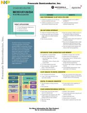
A FLASH MCU SOLUTION
MC9S12E128/E64
16-bit Microcontroller
The HCS12 Family of microcontrollers
is the next generation of the highly
successful 68HC12 architecture. Utilizing
Motorola’s industry-leading 0.25µ Flash,
the E128 is part of a pin-compatible
family that is planned to scale from
32 Kbytes to 512 Kbytes of Flash
memory. The E128 provides an upward
migration path from Motorola’s 68HC08,
68HC11 and 68HC12 architectures
for applications that need larger
memory, more peripherals and
higher performance.
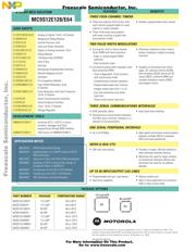
V reg 3.3 V to 5.5 V
LVI/LVR
16-Key Wakeup
IRQ Ports
PMF
6-ch
128K/64K Flash
8K RAM
DAC 0
ATD
10-bit
DAC 1
Timer 1
4-ch,
16-bit
Timer 2
4-ch,
16-bit
Timer 3
4-ch,
16-bit
PWM
6-ch, 8-bit / 3-ch, 16-bit
HCS12 CPU
3 x SCI
SPI
Internal Bus
• Power Management Applications
• Industrial Controls
• Commercial Controls
Frees
cale Semiconductor,
I
Freescale Semiconductor, Inc.
For More Information On This Product,
Go to: www.freescale.com
nc...
Verzeichnis
- ・ Technische Daten on Seite 2
- ・ Anwendungsbereich on Seite 1