
herunterladen
© Semiconductor Components Industries, LLC, 2007
February, 2007 − Rev. 17
1 Publication Order Number:
MC74VHC1G86/D
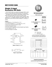
MC74VHC1G86
Single 2−Input
Exclusive OR Gate
The MC74VHC1G86 is an advanced high speed CMOS 2−input
Exclusive OR gate fabricated with silicon gate CMOS technology.
The internal circuit is composed of three stages, including a buffer
output which provides high noise immunity and stable output.
The MC74VHC1G86 input structure provides protection when
voltages up to 7 V are applied, regardless of the supply voltage. This
allows the MC74VHC1G86 to be used to interface 5 V circuits to 3 V
circuits.
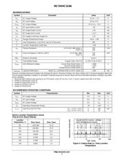
Features
• High Speed: t
PD
= 3.5 ns (Typ) at V
CC
= 5 V
• Low Power Dissipation: I
CC
= 1 mA (Max) at T
A
= 25°C
• Power Down Protection Provided on Inputs
• Balanced Propagation Delays
• Pin and Function Compatible with Other Standard Logic Families
• Chip Complexity: FETs = 54
• Pb−Free Packages are Available
Figure 1. Pinout (Top View)
V
CC
IN B
IN A
OUT Y
GND
IN A
IN B
OUT Y
= 1
Figure 2. Logic Symbol
1
2
3
5
4
http://onsemi.com
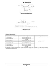
ORDERING INFORMATION
See detailed ordering and shipping information in the package
dimensions section on page 4 of this data sheet.
L
L
H
H
L
H
L
H
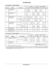
FUNCTION TABLE
Inputs Output
AB
L
H
H
L
Y
PIN ASSIGNMENT
1
2
3 GND
IN B
IN A
4
5V
CC
OUT Y
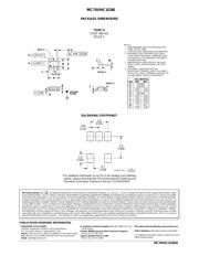
MARKING
DIAGRAMS
V8 = Device Code
M = Date Code*
G = Pb−Free Package
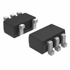
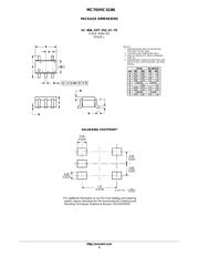
SC−88A / SOT−353 / SC−70
DF SUFFIX
CASE 419A
TSOP−5 / SOT−23 / SC−59
DT SUFFIX
CASE 483
V8 M G
G
(Note: Microdot may be in either location)
*Date Code orientation and/or position may
vary depending upon manufacturing location.
1
5
V8 M G
G
M
Verzeichnis
- ・ Konfiguration des Pinbelegungsdiagramms on Seite 1
- ・ Abmessungen des Paketumrisses on Seite 5 Seite 6
- ・ Paket-Footprint-Pad-Layout on Seite 5 Seite 6
- ・ Teilenummerierungssystem on Seite 1 Seite 4 Seite 6
- ・ Markierungsinformationen on Seite 1
- ・ Technische Daten on Seite 4
- ・ Elektrische Spezifikation on Seite 3