

herunterladen
© Semiconductor Components Industries, LLC, 2011
August, 2011 − Rev. 2
1 Publication Order Number:
AND9005/D
AND9005/D
Use of MC33161 Pspice
Model
Prepared by: Gang Chen
ON Semiconductor
Overview
The MC33161 is a universal voltage monitor intended for
use in a wide variety of voltage sensing applications. This
device offers the circuit designer an economical solution for
positive and negative voltage detection. The circuit consists
of two comparator channels each with hysteresis, a unique
Mode Select Input for channel programming, a pinned out
2.54 V reference, and two open collector outputs capable of
sinking in excess of 10 mA. Each comparator channel can be
configured as either inverting or non-inverting by the Mode
Select Input. This allows over, under, and window detection
of positive and negative voltages. The minimum supply
voltage needed for these devices to be fully functional is
2.0 V for positive voltage sensing and 4.0 V for negative
voltage sensing.
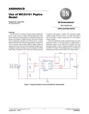
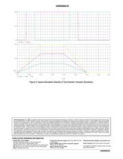
To provide simulation results and initial design of system
parameters before a real board design in applications, a
simulation model of the MC33161 in Pspice has been
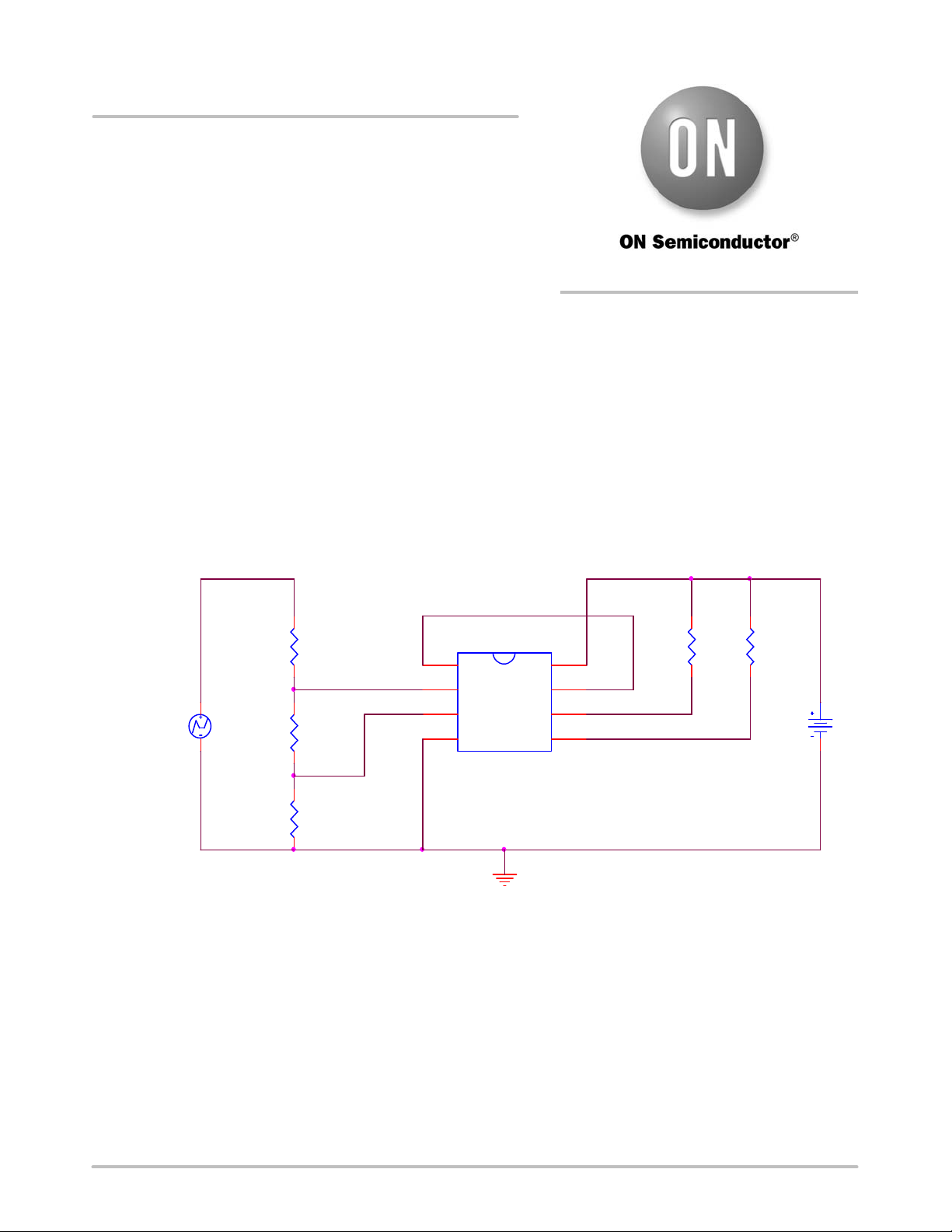
developed. Figure 1 shows a typical simulation circuit with
the MC33161 model. This simulation note is to illustrate a
simulation procedure with the MC33161 Pspice model.
0
R3
10k
R2
10k
R1
10k
R4
10k
IN1
V1
5Vdc
V2
T1 = 0
T2 = 1u
T3 = 2u
T4 = 3u
V1 = 0
V2 = 5
V3 = 5
V4 = 0
Vs
R5
10kU1
MC33161
VREF
1
IN1
2
IN2
3
GND
4
OUT2
5
OUT1
6
MODE
7
VCC
8
IN2
VCC
Vmode
Vout1
Vout2
Figure 1. Typical Simulation Circuit with MC33161 Pspice Model
http://onsemi.com
APPLICATION NOTE
Verzeichnis
- ・ Teilenummerierungssystem on Seite 5
- ・ Blockdiagramm on Seite 3