
herunterladen
© Semiconductor Components Industries, LLC, 2014
July, 2014 − Rev. 8
1 Publication Order Number:
MC14526B/D
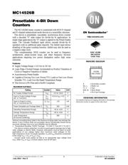
MC14526B
Presettable 4-Bit Down
Counters
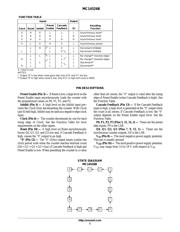
The MC14526B binary counter is constructed with MOS P−channel
and N−channel enhancement mode devices in a monolithic structure.
This device is presettable, cascadable, synchronous down counter
with a decoded “0” state output for divide−by−N applications. In
single stage applications the “0” output is applied to the Preset Enable
input. The Cascade Feedback input allows cascade divide−by−N
operation with no additional gates required. The Inhibit input allows
disabling of the pulse counting function. Inhibit may also be used as
a negative edge clock.
This complementary MOS counter can be used in frequency
synthesizers, phase−locked loops, and other frequency division
applications requiring low power dissipation and/or high noise
immunity.
Features
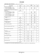
• Supply Voltage Range = 3.0 Vdc to 18 Vdc
• Logic Edge−Clocked Design: Incremented on Positive Transition of
Clock or Negative Transition of Inhibit
• Asynchronous Preset Enable
• Capable of Driving Two Low−Power TTL Loads or One Low−Power
Schottky TTL Load Over the Rated Temperature Range
• This Device is Pb−Free and is RoHS Compliant
MAXIMUM RATINGS
Rating Symbol Value Unit
DC Supply Voltage Range V
DD
−0.5 to +18.0 V
Input or Output Voltage Range
(DC or Transient)
V
in
,
V
out
−0.5 to V
DD
+ 0.5 V
Input or Output Current
(DC or Transient) per Pin
I
in
, I
out
±10 mA
Power Dissipation per Package (Note 1) P
D
500 mW
Operating Temperature Range T
A
−55 to +125 °C
Storage Temperature Range T
stg
−65 to +150 °C
Lead Temperature
(8−Second Soldering)
T
L
260 °C
Stresses exceeding those listed in the Maximum Ratings table may damage the
device. If any of these limits are exceeded, device functionality should not be
assumed, damage may occur and reliability may be affected.
1. Temperature Derating: “D/DW” Package: –7.0 mW/_C From 65_C To 125_C
This device contains protection circuitry to guard against damage due to high
static voltages or electric fields. However, precautions must be taken to avoid
applications of any voltage higher than maximum rated voltages to this
high−impedance circuit. For proper operation, V
in
and V
out
should be constrained
to the range V
SS
≤ (V
in
or V
out
) ≤ V
DD
.
Unused inputs must always be tied to an appropriate logic voltage level
(e.g., either V
SS
or V
DD
). Unused outputs must be left open.
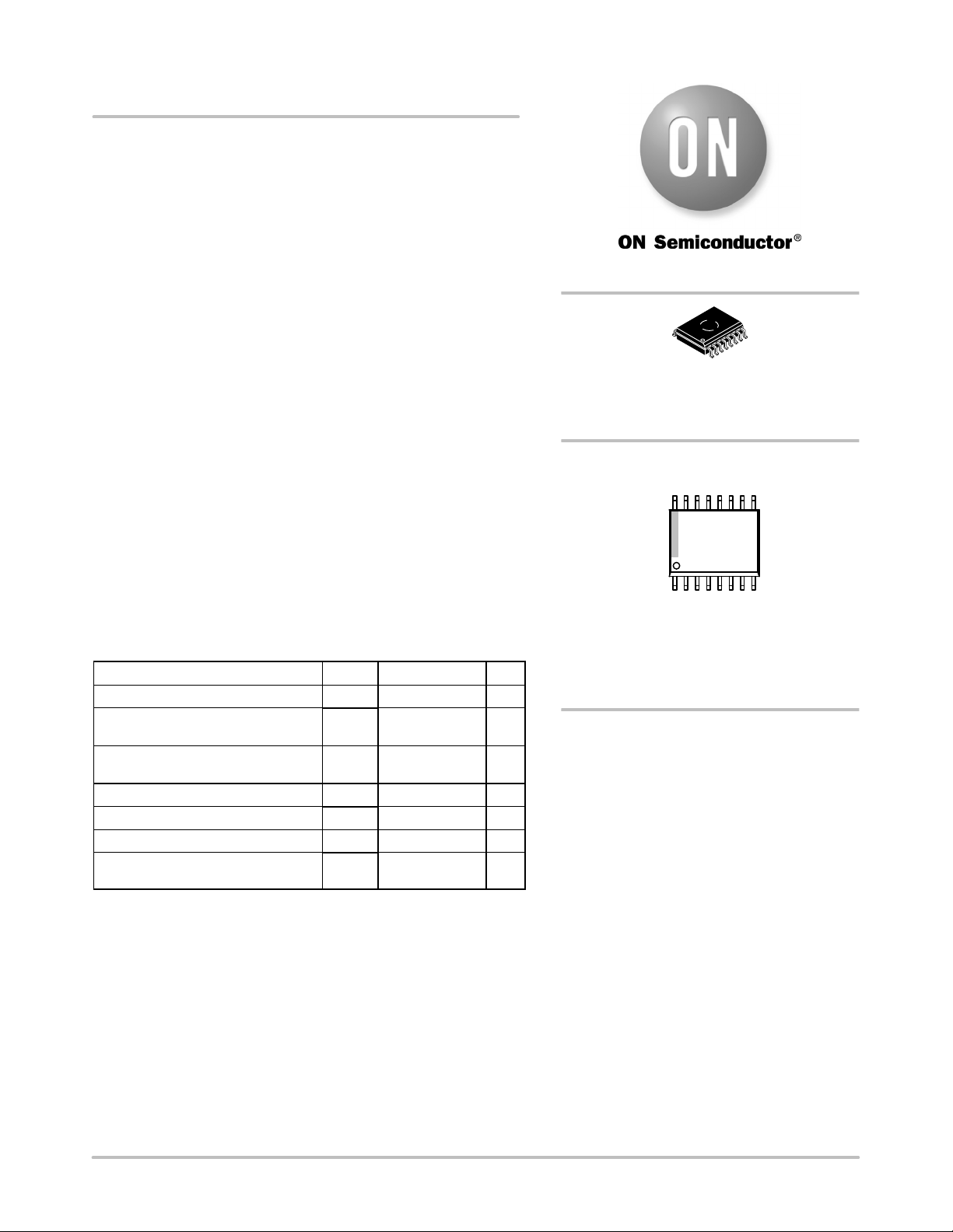
http://onsemi.com
See detailed ordering and shipping information in the package
dimensions section on page 8 of this data sheet.
ORDERING INFORMATION
SOIC−16 WB
DW SUFFIX
CASE 751G
MARKING DIAGRAM
A = Assembly Location
WL, L = Wafer Lot
YY, Y = Year
WW, W = Work Week
G = Pb−Free Package
1
1
14526B
AWLYWWG
Verzeichnis
- ・ Konfiguration des Pinbelegungsdiagramms on Seite 2
- ・ Abmessungen des Paketumrisses on Seite 9
- ・ Paket-Footprint-Pad-Layout on Seite 9
- ・ Teilenummerierungssystem on Seite 1 Seite 8 Seite 9
- ・ Markierungsinformationen on Seite 1 Seite 9
- ・ Typisches Anwendungsschaltbild on Seite 7
- ・ Technische Daten on Seite 8
- ・ Anwendungsbereich on Seite 7
- ・ Elektrische Spezifikation on Seite 3
- ・ Teilenummernliste on Seite 1