
herunterladen

Maxim > Design Support > Technical Documents > Application Notes > Automotive > APP 3821
Maxim > Design Support > Technical Documents > Application Notes > High-Speed Interconnect > APP 3821
Maxim > Design Support > Technical Documents > Application Notes > High-Speed Signal Processing > APP 3821
Keywords: 21-bit multiple input channel deserializers, skew margin measurement, jitter tolerance, clock
jitter, data jitter, channel-to-channel skew, DC balance
APPLICATION NOTE 3821
Skew Margin Measurement for 4-Channel (3 Data
Channels Plus Clock Channel) LVDS
Serializers/Deserializers
Jun 20, 2006
Abstract: Measuring receiver skew margin is a practical way to determine the jitter tolerance of multiple-
input-channel LVDS deserializers like the MAX9209/MAX9222 parts. Although receiver skew margin has
been defined and explained in the literature, no comprehensive measurement technique has yet been
demonstrated. This application note shows a step-by-step method for measuring skew margin. Following
this approach, you can clarify the specification and definition of skew margin in the data sheets for these
4-channel SerDes devices.
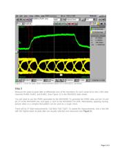
The following measurements were performed in several steps and using the MAX9209/MAX9222
serializer/deserializer (SerDes) parts in DC-balance mode with a 10m shielded twisted-pair cable. In all
measurements, a Tektronix P6248 FET differential probe and a Tektronix CSA8000 sampling
oscilloscope were used. A PRBS data pattern was used.
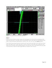
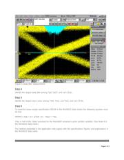
Step 1
Make the peak-to-peak jitter measurement at 0V differential on the rising edge of RxCLKIN. Call it Tjclk.
(See Figure 1.)
Page 1 of 5