
herunterladen

Maxim > Design Support > Technical Documents > Application Notes > High-Speed Interconnect > APP 3662
Keywords: LVDS receiver, failsafe function, uncertain output state, open input, float input, improper
connection, external-biasing failsafe, in-path failsafe, and parallel failsafe
APPLICATION NOTE 3662
Understanding LVDS Fail-Safe Circuits
Mar 22, 2006
Abstract: Low-voltage differential signaling (LVDS) is a widely used differential signaling technology for
high-speed digital-signal interconnections. In many applications, the LVDS receiver needs a fail-safe
function to avoid an uncertain output state when the input is connected improperly. In this application
note, we will examine the circuit design and performance characteristics of three popular fail-safe
functions. Comparative analysis of circuit designs will guide readers in the use of fail-safe circuits for
high-speed data-transfer applications.
Introduction
In recent years low-voltage differential signaling (LVDS)
[1]
for high-speed data interconnections has
found broad application in consumer electronics, high-speed computer peripherals, telecom/networking,
and wireless base stations. LVDS has distinctive advantages in performance, power, noise, EMI
reduction, and cost. With appropriate settings, at a data rate of 100Mbps to 800Mbps the LVDS signal
can reach as far as 10m to 15m in a twisted-pair cable link, or > 1m in a PCB trace pair. The power
dissipated by the 100Ω load is a mere 1.2mW relatively independent of frequency.
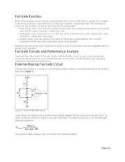
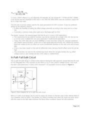
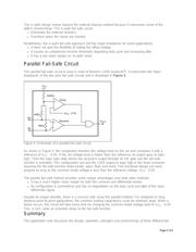
This application note discusses the LVDS fail-safe function, which is very important for appropriate LVDS
operation. We will examine three fail-safe circuits, analyze their characteristics, and provide guidance for
applications.
Basic Characteristics and Advantages of LVDS
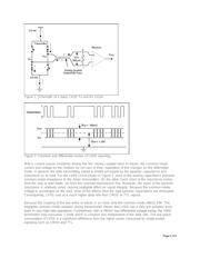
Let us briefly review the basic structure of the LVDS signaling and circuit configuration. Figure 1 shows
a simple, basic circuit for LVDS transmission and receiving. The receiver is a comparator with an
absolute transition threshold of about 50mV. The transmission media, whether cable or PCB trace pair,
are designed with a 100Ω differential impedance. Figure 2 shows the signal levels for both common and
differential modes on the media. In Figures 1 and 2, V
ID
is the input differential voltage of the LVDS
receiver, V
OD
is the differential output voltage of the LVDS transmitter, and V
CM
is the common-mode
voltage.
Page 1 of 6