
herunterladen
Maxim > Design Support > Technical Documents > Application Notes > Digital Potentiometers > APP 4221
Maxim > Design Support > Technical Documents > Application Notes > Optoelectronics > APP 4221
Maxim > Design Support > Technical Documents > Application Notes > Power-Supply Circuits > APP 4221
Keywords: APD, bias, DS1841, temperature compensation, boost, step-up
APPLICATION NOTE 4221
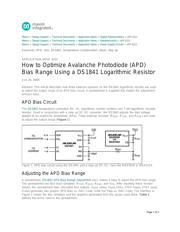
How to Optimize Avalanche Photodiode (APD)
Bias Range Using a DS1841 Logarithmic Resistor
Jun 10, 2008
Abstract: This article describes how three external resistors on the DS1841 logarithmic resistor are used
to adjust the output range of an APD bias circuit. A spreadsheet is supplied that makes the adjustment
process easy.
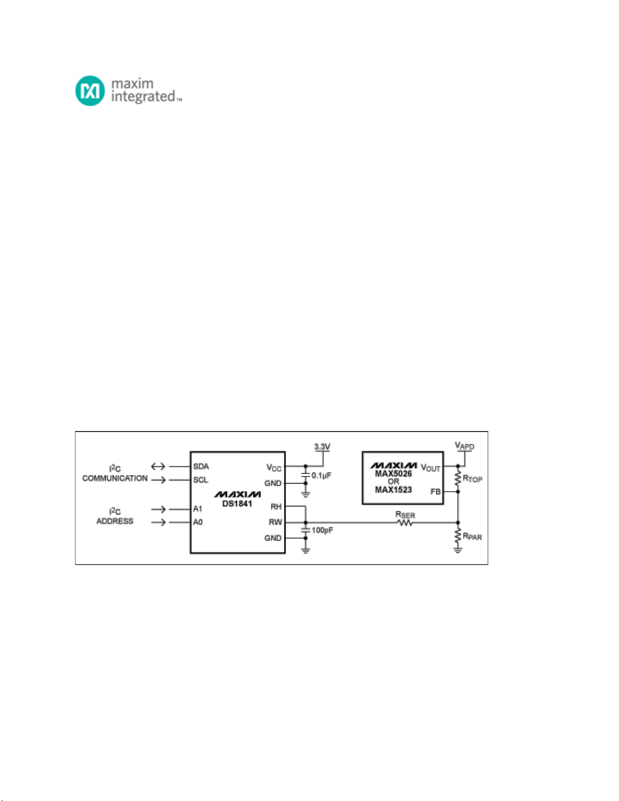
APD Bias Circuit
The DS1841 temperature-controlled, NV, I²C, logarithmic resistor contains one 7-bit logarithmic variable
resistor. Used in conjunction with a step-up DC-DC converter, the DS1841 adjusts the bias voltage
applied to an avalanche photodiode (APD). Three external resistors (R
SER
, R
TOP
, and R
PAR
) are used
to adjust the output range (Figure 1).
Figure 1. APD bias circuit using the DS1841 and a step-up DC-DC, here the MAX5026 or MAX1523.
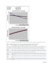
Adjusting the APD Bias Range
A spreadsheet, DS1841 APD Bias Range Adjustment (xls), makes it easy to adjust the APD bias range.
The spreadsheet has four input variables: R
TOP
, R
SER
, R
PAR
, and V
FB
. After inputting these resistor
values, the spreadsheet then calculates four outputs: V
APD
(max), V
APD
(min), STEP (max), STEP (avg).
It also generates two graphs: APD Bias vs. DAC Code, Volts Per Step vs. DAC Code. The interface in
Figure 2 shows the four variables and the graphics generated from the values input there. Table 1
defines the terms used in the spreadsheet.
Page 1 of 3