
herunterladen
Maxim > Design Support > Technical Documents > Application Notes > A/D and D/A Conversion/Sampling Circuits > APP 1948
Keywords: ADC, analog to digital converter, voltage divider, distortion, gain error, high impedance, low
impedance, sampling capacitor, time constant, a/d converters
APPLICATION NOTE 1948
Analysis of ADC System Distortion Caused by
Source Resistance
Mar 25, 2003
Abstract: Analog-to-digital converter (ADC) data sheets and application typically recommend driving their
inputs with a low source impedance. This application note explains the possible effects such as increased
gain error and distortion when using high impedance to drive an ADC without a buffer.
Analog-to-digital converter (ADC) users have been instructed by endless data sheets and application
notes to drive their ADCs with a low source impedance. However, these instructions often do not tell us
what can happen if a low impedance is not used and what effects it can have on circuit performance. This
article explains the principles behind and techniques for understanding the source of the distortion caused
from a high source resistance on the input to an analog-to-digital converter.
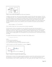
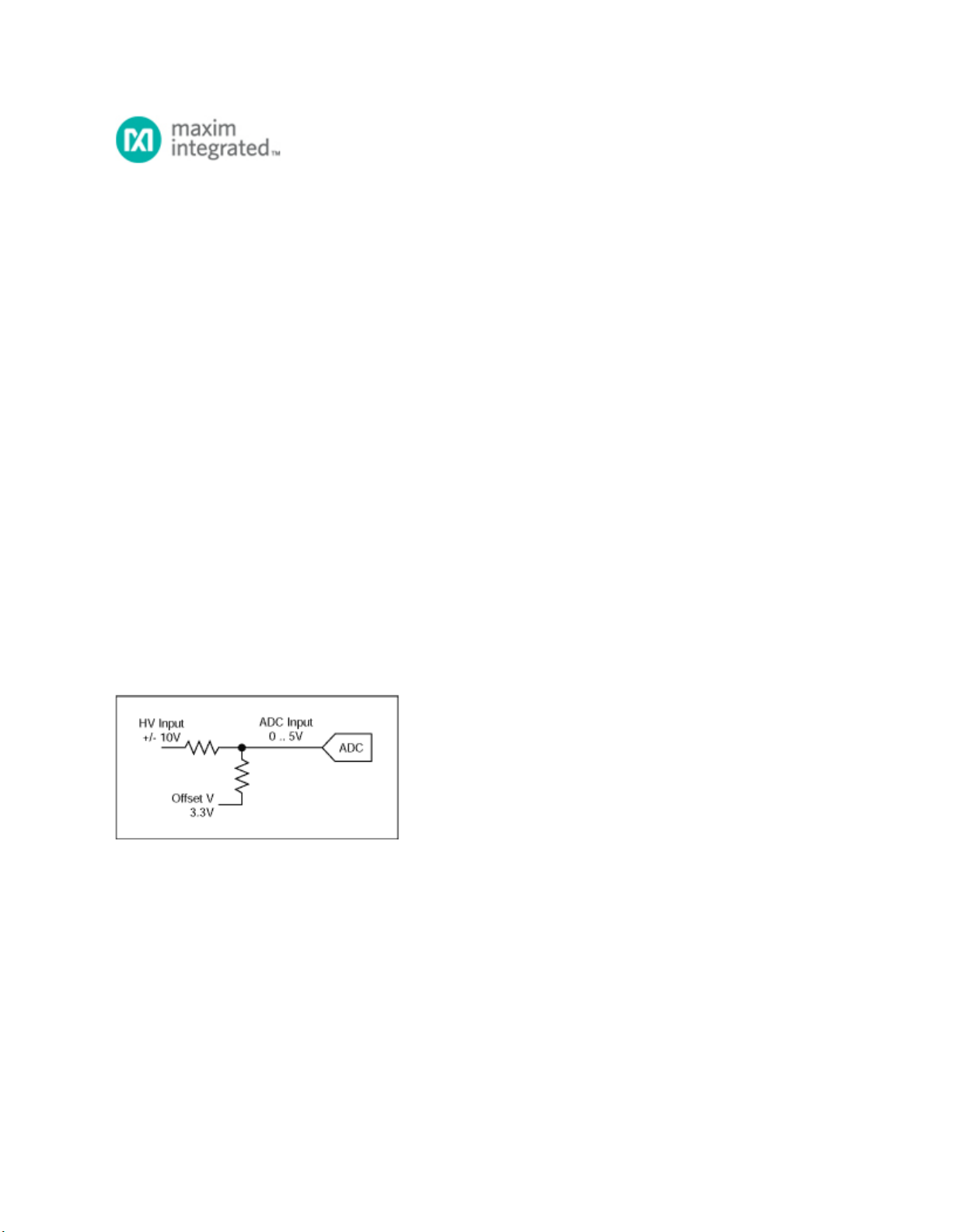
We can begin to understand the problem of high-source impedance effects by looking at the simple circuit
below in Figure 1. It addresses a common need to scale a ±10V signal to a 0 to 5V ADC input with a
simple voltage divider.
Figure 1. Scaling ADC input with a simple voltage divider.
For this circuit, the effective driving impedance into the ADC is the Thevenin equivalent impedance seen
looking back into the divider, which equals the parallel combination of the divider resistors. This finite
input resistance acts as a voltage divider with the input impedance of the ADC causing a low-frequency
gain error as shown in Figure 2.
Page 1 of 5