

herunterladen
Semiconductor Components Industries, LLC, 2005
May, 2005 − Rev. 11
1 Publication Order Number:
MC74VHC1GT126/D
MC74VHC1GT126
Noninverting Buffer /
CMOS Logic Level Shifter
with LSTTL−Compatible Inputs
The MC74VHC1GT126 is a single gate noninverting 3−state buffer
fabricated with silicon gate CMOS technology. It achieves high speed
operation similar to equivalent Bipolar Schottky TTL while maintaining
CMOS low power dissipation.
The MC74VHC1GT126 requires the 3−state control input (OE) to be
set Low to place the output into the high impedance state.
The device input is compatible with TTL−type input thresholds and the
output has a full 5.0 V CMOS level output swing. The input protection
circuitry on this device allows overvoltage tolerance on the input,
allowing the device to be used as a logic−level translator from 3.0 V
CMOS logic to 5.0 V CMOS Logic or from 1.8 V CMOS logic to 3.0 V
CMOS Logic while operating at the high−voltage power supply.
The MC74VHC1GT126 input structure provides protection when
voltages up to 7.0 V are applied, regardless of the supply voltage. This
allows the MC74VHC1GT126 to be used to interface 5.0 V circuits to
3.0 V circuits. The output structures also provide protection when V
CC
=
0 V. These input and output structures help prevent device destruction
caused by supply voltage − input/output voltage mismatch, battery
backup, hot insertion, etc.
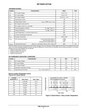
Features
• High Speed: t
PD
= 3.5 ns (Typ) at V
CC
= 5.0 V
• Low Power Dissipation: I
CC
= 1 A (Max) at T
A
= 25°C
• TTL−Compatible Inputs: V
IL
= 0.8 V; V
IH
= 2.0 V
• CMOS−Compatible Outputs: V
OH
> 0.8 V
CC
; V
OL
< 0.1 V
CC
@Load
• Power Down Protection Provided on Inputs and Outputs
• Balanced Propagation Delays
• Pin and Function Compatible with Other Standard Logic Families
• Chip Complexity: FETs = 62; Equivalent Gates = 16
• Pb−Free Packages are Available
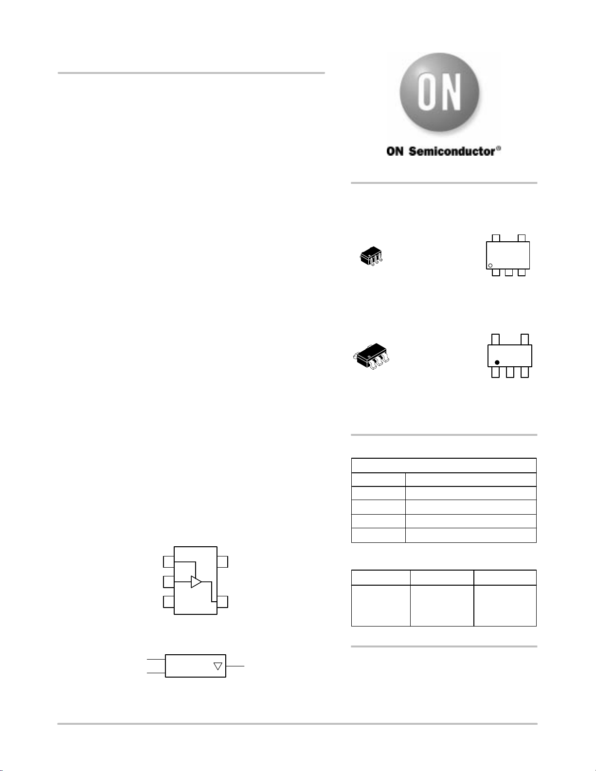
Figure 1. Pinout (Top View)
IN A
OUT Y
V
CC
OE
IN A
OUT YGND
OE
Figure 2. Logic Symbol
1
2
3
4
5
PIN ASSIGNMENT
1
2
3 GND
OE
IN A
4
5V
CC
OUT Y
See detailed ordering and shipping information in the package
dimensions section on page 4 of this data sheet.
ORDERING INFORMATION
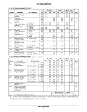
FUNCTION TABLE
L
H
X
A Input Y Output
L
H
Z
OE Input
H
H
L
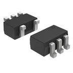
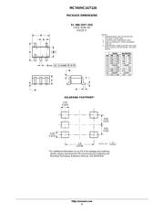
SC−88A/SOT−353/SC−70
DF SUFFIX
CASE 419A
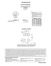
TSOP−5/SOT−23/SC−59
DT SUFFIX
CASE 483
MARKING
DIAGRAMS
http://onsemi.com
1
5
W3AWW
A = Assembly Location
WW = Work Week
= Pb−Free Package
(Note: Microdot may be in either location)
1
5
W3 M
M = Date Code
= Pb−Free Package
(Note: Microdot may be in either location)
Verzeichnis
- ・ Konfiguration des Pinbelegungsdiagramms on Seite 1
- ・ Abmessungen des Paketumrisses on Seite 5 Seite 6
- ・ Paket-Footprint-Pad-Layout on Seite 5 Seite 6
- ・ Teilenummerierungssystem on Seite 1 Seite 4 Seite 6
- ・ Markierungsinformationen on Seite 1
- ・ Technische Daten on Seite 4
- ・ Elektrische Spezifikation on Seite 3