
herunterladen
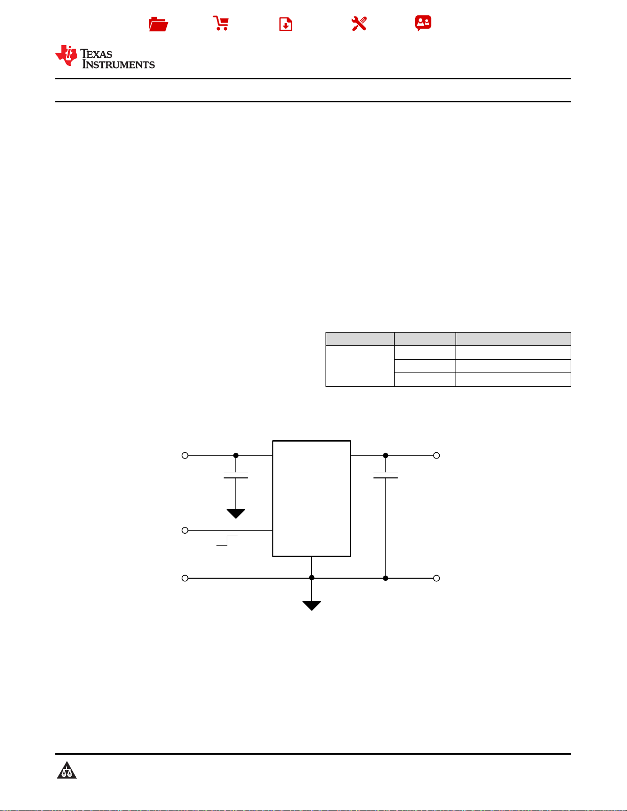
EN
IN OUT
GND
V
IN
V
EN
GND
V
OUT
LP3990
C
OUT
1 µF
C
IN
1 µF
OFF
ON
GND
Product
Folder
Sample &
Buy
Technical
Documents
Tools &
Software
Support &
Community
LP3990
SNVS251J –MAY 2004–REVISED SEPTEMBER 2014
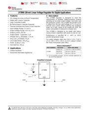
LP3990 150-mA Linear Voltage Regulator for Digital Applications
1 Features 3 Description
The LP3990 regulator is designed to meet the
1
• 1% Voltage Accuracy at Room Temperature
requirements of portable, battery-powered systems
• Stable with Ceramic Capacitor
providing an accurate output voltage, low-noise, and
• Logic Controlled Enable
low-quiescent current. The LP3990 will provide a 0.8-
V output from the low input voltage of 2 V at up to a
• No Noise Bypass Capacitor Required
150-mA load current. When switched into shutdown
• Thermal-Overload and Short-Circuit Protection
mode via a logic signal at the enable pin (EN), the
• Input Voltage Range, 2 V to 6 V
power consumption is reduced to virtually zero.
• Output Voltage Range, 0.8 V to 3.3 V
The LP3990 is designed to be stable with space-
• Output Current, 150 mA
saving ceramic capacitors with values as low as 1 µF.
• Output Stable - Capacitors, 1 µF
Performance is specified for a –40°C to 125°C
• Virtually Zero I
Q
(Disabled), < 10 nA
junction temperature range.
• Very Low I
Q
(Enabled), 43 µA
For output voltages other than 0.8 V, 1.2 V, 1.35 V,
• Low Output Noise, 150 µV
RMS
1.5 V, 1.8 V, 2.5 V, 2.8 V, or 3.3 V, please contact
the Texas Instruments sales office.
• PSRR, 55 dB at 1 kHz
• Fast Start-Up, 105 µs
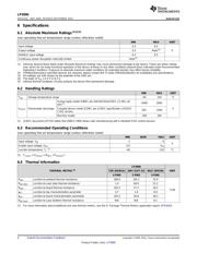
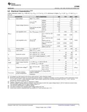
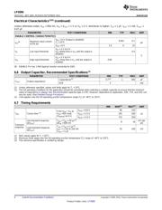
Device Information
(1)
PART NUMBER PACKAGE BODY SIZE (NOM)
2 Applications
DSBGA (4) 1.324 mm x 1.045 mm (MAX)
• Cellular Handsets
LP3990 WSON (6) 2.90 mm x 1.60 mm
• Hand-Held Information Appliances
SOT-23 (5) 3.00 mm x 3.00 mm
(1) For all available packages, see the orderable addendum at
the end of the datasheet.
Simplified Schematic
1
An IMPORTANT NOTICE at the end of this data sheet addresses availability, warranty, changes, use in safety-critical applications,
intellectual property matters and other important disclaimers. PRODUCTION DATA.
Verzeichnis
- ・ Konfiguration des Pinbelegungsdiagramms on Seite 3
- ・ Abmessungen des Paketumrisses on Seite 18 Seite 19 Seite 21 Seite 22 Seite 23
- ・ Markierungsinformationen on Seite 18 Seite 19 Seite 20
- ・ Blockdiagramm on Seite 1 Seite 9
- ・ Typisches Anwendungsschaltbild on Seite 11
- ・ Technische Daten on Seite 4 Seite 6
- ・ Anwendungsbereich on Seite 1 Seite 28
- ・ Elektrische Spezifikation on Seite 5 Seite 6 Seite 7 Seite 8 Seite 14