
herunterladen
© Semiconductor Components Industries, LLC, 2012
December, 2012 − Rev. 0
1 Publication Order Number:
AND9116/D
AND9116/D
Latch-up Considerations for
ESD Protection Devices on
High Speed Serial Interface
Applications
Introduction
As process geometries of chipsets that drive today’s high
speed serial interfaces become smaller and consequently
more sensitive to transients such as ESD, the challenge to
provide adequate protection for these chipsets is growing. A
type of device that exhibits a negative resistance on a portion
of their current−voltage characteristic is one solution to
overcome the protection challenge. However, when using
such a snap-back device, the effect of data line latch−up must
be considered. This application note will discuss the effects
of a latch−up condition and their applicability to snap-back
protection devices. The note will also explain the relevant
portions of certain high speed serial interfaces such as
HDMI 1.4, USB 2.0, and USB 3.0 with respect to latch-up
by analyzing potential latch−up conditions in each case.
Based on the analysis, recommendations and design
specifications for the protection device will be presented for
each case in order to guarantee latch−up free applications.
The below recommendations for each case will be discussed
in relation to ON Semiconductor’s ESD8000 series
technology.
Latch−Up Effects
A latch−up condition may be initiated by a transient (such
as ESD, conducted or radiated EMI, or surge) bringing the
protection device into conduction. Latch−up is said to occur
if the device remains in an on state, after the transient has
passed. The latch−up state can be maintained in a snapback
device if the power source on the protection can supply
enough voltage and current to maintain the protection
device’s on state.
Latch−up conditions are not desirable because of two
main reasons. One being that the conduction current may be
excessive, thus causing damage to the protection device, the
application circuit, or both from the resulting power
dissipation. The other being that the voltage across the
protection device in conduction may be too low to allow the
application circuit node to reach its normally intended
voltage.
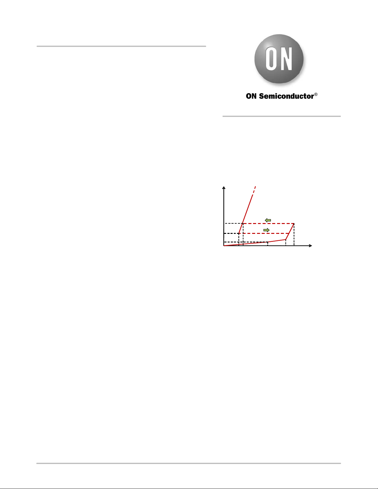
Latch−Up Free Design: General Approach
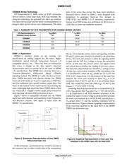
Figure 1 shows the typical current−voltage characteristic
of a snap−back protection device (such as a silicon
controlled rectifier or SCR for example). The parameters of
interest as shown on Figure 1 are: the breakdown voltage
(V
BR
), break−over voltage (V
BO
), snap−back voltage
(V
SB
), and both the holding current (I
H
) and holding voltage
(V
H
).
I
V
V
RWM
V
BO
V
SB
V
H
I
L
I
H
I
BO
V
BR
Figure 1. Typical Snap−back Protection Device
Current−Voltage Characteristic
Several parameters of the protection device can be acted
upon to prevent a latch−up condition. The protection device
snap−back voltage (V
SB
) can be designed to be higher than
the maximum operating voltage, V
SS
or V
RWM
, of the
application line. In this case, every point of the
current−voltage characteristic is above the maximum
operating voltage, for currents above the leakage level I
L
.
This is representative of standard Zener diode protection
devices for example which do not exhibit snap−back
characteristics. Another key parameter that can be designed
to prevent a latch−up condition is the holding current, I
H
.
The holding current can be designed to be higher than the
maximum steady−state current I
SSMAX
the application
circuit can supply. While these serve as guidelines that will
guarantee latch−up free designs under all circumstances,
they can be overly conservative. A load−line analysis of the
application circuit can provide more refined guidelines,
which will allow a better tuning of the protection device
characteristics.
Latch−Up Free Design: Load−Line Approach
The load-line analysis of the application circuit assumes
that its behavior is linear, and that the source can be
http://onsemi.com
APPLICATION NOTE
Verzeichnis