
herunterladen
Altera Corporation Section I–1
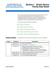
Section I. Stratix Device
Family Data Sheet
This section provides the data sheet specifications for Stratix
®
devices.
They contain feature definitions of the internal architecture,
configuration and JTAG boundary-scan testing information, DC
operating conditions, AC timing parameters, a reference to power
consumption, and ordering information for Stratix devices.
This section contains the following chapters:
■ Chapter 1, Introduction
■ Chapter 2, Stratix Architecture
■ Chapter 3, Configuration & Testing
■ Chapter 4, DC & Switching Characteristics
■ Chapter 5, Reference & Ordering Information
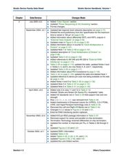
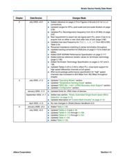
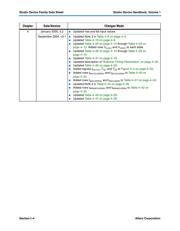
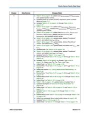
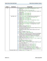
Revision History
The table below shows the revision history for Chapters 1 through 5.
Chapter Date/Version Changes Made
1 July 2005, v3.2 ● Minor content changes.
September 2004, v3.1
● Updated Table 1–6 on page 1–5.
April 2004, v3.0
● Main section page numbers changed on first page.
● Changed PCI-X to PCI-X 1.0 in “Features” on page 1–2.
● Global change from SignalTap to SignalTap II.
● The DSP blocks in “Features” on page 1–2 provide dedicated
implementation of multipliers that are now “faster than 300 MHz.”
January 2004, v2.2
● Updated -5 speed grade device information in Table 1-6.
October 2003, v2.1
● Add -8 speed grade device information.
July 2003, v2.0
● Format changes throughout chapter.
Verzeichnis
- ・ Konfiguration des Pinbelegungsdiagramms on Seite 91 Seite 92
- ・ Abmessungen des Paketumrisses on Seite 275
- ・ Teilenummerierungssystem on Seite 275 Seite 276
- ・ Blockdiagramm on Seite 16 Seite 69 Seite 70
- ・ Typisches Anwendungsschaltbild on Seite 20 Seite 22 Seite 24 Seite 26
- ・ Beschreibung der Funktionen on Seite 15 Seite 16
- ・ Technische Daten on Seite 3 Seite 171 Seite 173 Seite 174 Seite 176
- ・ Anwendungsbereich on Seite 190 Seite 191
- ・ Elektrische Spezifikation on Seite 168