


herunterladen
Application Report
SLPA010 – November 2011
1
Ringing Reduction Techniques for
NexFET
TM
High Performance MOSFETs
ABSTRACT
The design of switching converters with high performance MOSFET’s such as those found in the NexFET
TM
product line
require special attention to detail to maximize the effectiveness of the devices and optimize the overall performance of the
switching function. Consideration of the challenges of working with ultra-fast power devices early in the design process will
ensure the highest performing, most reliable final product.
In this Application Note, the Power Stage of the typical Non-Isolated Synchronous Buck Converter (see Figure 1) will be
used as a reference for discussing practical design considerations for maximizing the performance and lifetime of NexFET
products. The most common problem encountered in this scenario is parasitic Voltage Ringing superimposed on the rising
edge of the Switch Node.
This Application Note will discuss the source of the switch node ringing, measurement techniques to accurately characterize
this ringing, and methods for minimizing the effect while maintaining excellent system performance.
Backgound
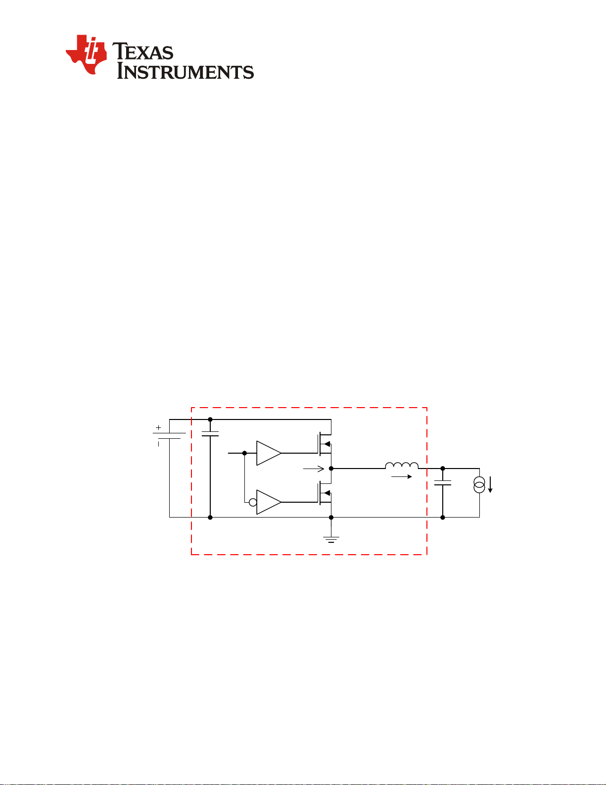
Figure 1 shows the schematic of a typical synchronous buck converter. As the performance of power devices is improved,
the control FET has the ability to switch voltages at rates greater than 10kV/µs. However, the fast switching faces a common
challenge of dealing with switching noise. In particular when the Control FET turns on and the Sync FET is off, the loop
inductor, the loop resistor and the output capacitor of the sync FET form a series RLC loop and will resonate at a resonant
frequency. This resonance will result in voltage overshoot and ringing at the switch node.
PWM
Control
FET
Sync
FET
Input
Supply
L
O
I
L
C
O
Load
Driver
Driver
C
I
Switch
Node
Figure 1. Definition of Power Stage Components
To understand the source of this ringing, it is useful to make a detailed examination of the switching transient. Assume the
Control FET is off, the Sync FET is on, all voltage transients have settled, but I
L
continues to flow (slewing at a constant
rate) (see Stage 1 in Figure2). During Stage 2, the Sync FET is turned off and a short deadtime is imposed to prevent shoot-
through before the Control FET is turned on. During the deadtime the inductor current forces the body diode of the Sync
FET to turn on, resulting in a slight drop in voltage at the Switch Node. Stage 3 is initiated by the turn on of the Control
FET. As current builds in the Control FET (limited by parasitic inductance and the on resistance of the FET), the body diode
of the Sync FET is forced off. The reverse recovery effect of the diode and the slewing of the FET capacitor voltages result
in overshoot of the Control FET current.
NexFET is a Trademark of Texas Instruments
Verzeichnis
- ・ Blockdiagramm on Seite 15
- ・ Anwendungsbereich on Seite 18