
herunterladen
© Semiconductor Components Industries, LLC, 2014
August, 2014 − Rev. 9
1 Publication Order Number:
MC14175B/D
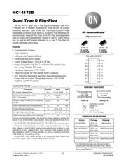
MC14175B
Quad Type D Flip-Flop
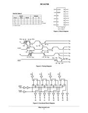
The MC14175B quad type D flip−flop is constructed with MOS
P−channel and N−channel enhancement mode devices in a single
monolithic structure. Each of the four flip−flops is positive−edge
triggered by a common clock input (C). An active−low reset input (R)
asynchronously resets all flip−flops. Each flip−flop has independent
Data (D) inputs and complementary outputs (Q and Q). These devices
may be used as shift register elements or as type T flip−flops for
counter and toggle applications.
Features
• Complementary Outputs
• Static Operation
• All Inputs and Outputs Buffered
• Diode Protection on All Inputs
• Supply Voltage Range = 3.0 Vdc to 18 Vdc
• Output Compatible with Two Low−Power TTL Loads or One
Low−Power Schottky TTL Load
• Functional Equivalent to TTL 74175
• These Devices are Pb−Free and are RoHS Compliant
• NLV Prefix for Automotive and Other Applications Requiring
Unique Site and Control Change Requirements; AEC−Q100
Qualified and PPAP Capable*
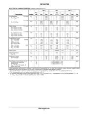
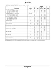
MAXIMUM RATINGS (Voltages Referenced to V
SS
)
Parameter
Symbol Value Unit
DC Supply Voltage Range V
DD
−0.5 to +18.0 V
Input or Output Voltage Range
(DC or Transient)
V
in
, V
out
−0.5 to V
DD
+ 0.5
V
Input or Output Current (DC or Transient)
per Pin
I
in
, I
out
±10 mA
Power Dissipation per Package (Note 1) P
D
500 mW
Ambient Temperature Range T
A
−55 to +125 °C
Storage Temperature Range −65 to +150 °C
Lead Temperature (8−Second Soldering) 260 °C
Stresses exceeding those listed in the Maximum Ratings table may damage the
device. If any of these limits are exceeded, device functionality should not be
assumed, damage may occur and reliability may be affected.
1. Temperature Derating: “D/DW” Packages: –7.0 mW/_C From 65_C To 125_C
This device contains protection circuitry to guard against damage due to high
static voltages or electric fields. However, precautions must be taken to avoid
applications of any voltage higher than maximum rated voltages to this
high−impedance circuit. For proper operation, V
in
and V
out
should be constrained
to the range V
SS
≤ (V
in
or V
out
) ≤ V
DD
.
Unused inputs must always be tied to an appropriate logic voltage level
(e.g., either V
SS
or V
DD
). Unused outputs must be left open.
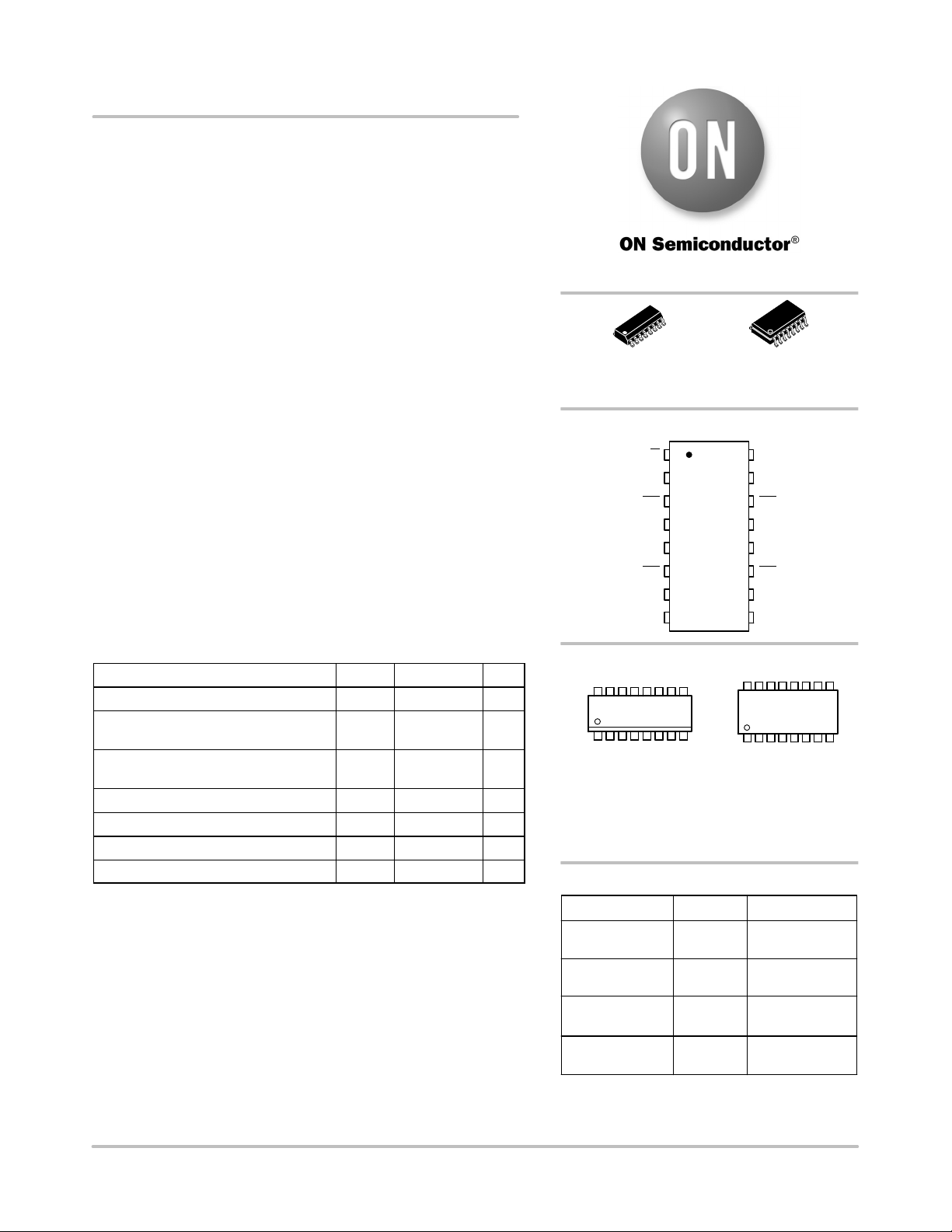
Device Package Shipping
†
ORDERING INFORMATION
http://onsemi.com
†For information on tape and reel specifications,
including part orientation and tape sizes, please
refer to our Tape and Reel Packaging Specification
s
Brochure, BRD8011/D.
MC14175BFELG SOEIAJ−16
(Pb−Free)
2000/Tape & Ree
l
MC14175BDR2G SOIC−16
(Pb−Free)
2500/Tape & Ree
l
MC14175BDG SOIC−16
(Pb−Free)
48 Units/Rail
A = Assembly Location
WL, L = Wafer Lot
YY, Y = Year
WW, W = Work Week
G = Pb−Free Package
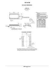
MARKING DIAGRAMS
SOIC−16
1
16
14175BG
AWLYWW
SOEIAJ−16
1
16
MC14175B
ALYWG
NLV14175BDR2G* SOIC−16
(Pb−Free)
2500/Tape & Ree
l
SOIC−16
D SUFFIX
CASE 751B
SOEIAJ−16
F SUFFIX
CASE 966
13
14
15
16
9
10
11
125
4
3
2
1
8
7
6
D2
D3
Q3
V
DD
C
Q2
Q2
D0
Q0
Q0
R
V
SS
Q1
Q1
D1
Q3
PIN ASSIGNMENT
Verzeichnis
- ・ Konfiguration des Pinbelegungsdiagramms on Seite 1
- ・ Abmessungen des Paketumrisses on Seite 5 Seite 6
- ・ Paket-Footprint-Pad-Layout on Seite 5
- ・ Teilenummerierungssystem on Seite 1 Seite 6
- ・ Markierungsinformationen on Seite 1 Seite 6
- ・ Blockdiagramm on Seite 2
- ・ Technische Daten on Seite 1
- ・ Anwendungsbereich on Seite 1
- ・ Elektrische Spezifikation on Seite 3
- ・ Teilenummernliste on Seite 1