
herunterladen
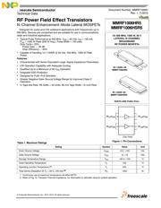
MMRF1006HR5 MMRF1006HSR5
1
RF Device Data
Freescale Semiconductor, Inc.
RF Power Field Effect Transistors
N--Channel Enhancement--Mode Lateral MOSFETs
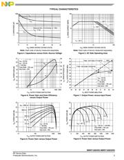
Designed for pulse and CW w ideband applications with frequencies up t o
500 MHz. Devices are unmatched and are suitable for use in communications,
radar and industrial applications.
• Typical Pulse Performance at 450 MHz: V
DD
=50Vdc,I
DQ
= 150 mA,
P
out
= 1000 W Peak (200 W Avg.), Pulse Width = 100 μsec,
Duty Cycle = 20%
Power Gain — 20 dB
Drain Efficiency — 64%
• Capable of Handling 10:1 VSWR @ 50 Vdc, 450 MHz, 1000 W Peak
Power
Features
• Characterized with Series Equivalent Large--Signal Impedance Parameters
• CW Operation Capability with Adequate Cooling
• Qualified Up to a Maximum of 50 V
DD
Operation
• Integrated ESD Protection
• Designed for Push--Pull Operation
• Greater Negative Gate--Source Voltage Range for Improved Class C
Operation
• In Tape and Reel. R5 Suffix = 50 Units, 56 mm Tape Width, 13--inch Reel.
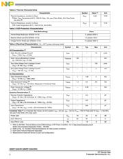
Table 1. Maximum Ratings
Rating Symbol Value Unit
Drain--Source Voltage V
DSS
--0.5, +120 Vdc
Gate--Source Voltage V
GS
-- 6 , + 1 0 Vdc
Storage Temperature Range T
stg
-- 65 to +150 °C
Case Operating Temperature T
C
150 °C
Operating Junction Temperature
(1)
T
J
225 °C
Total Device Dissipation @ T
C
=25°C, CW only
(2)
P
D
1333 W
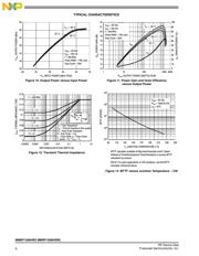
1. Continuous use at maximum temperature will affect MTTF.
2. Refer to Fig. 12, Transient Thermal Impedance, for information to calculate value for pulsed operation.
Document Number: MMRF1006H
Rev. 1, 11/2015
Freescale Semiconductor
Technical Data
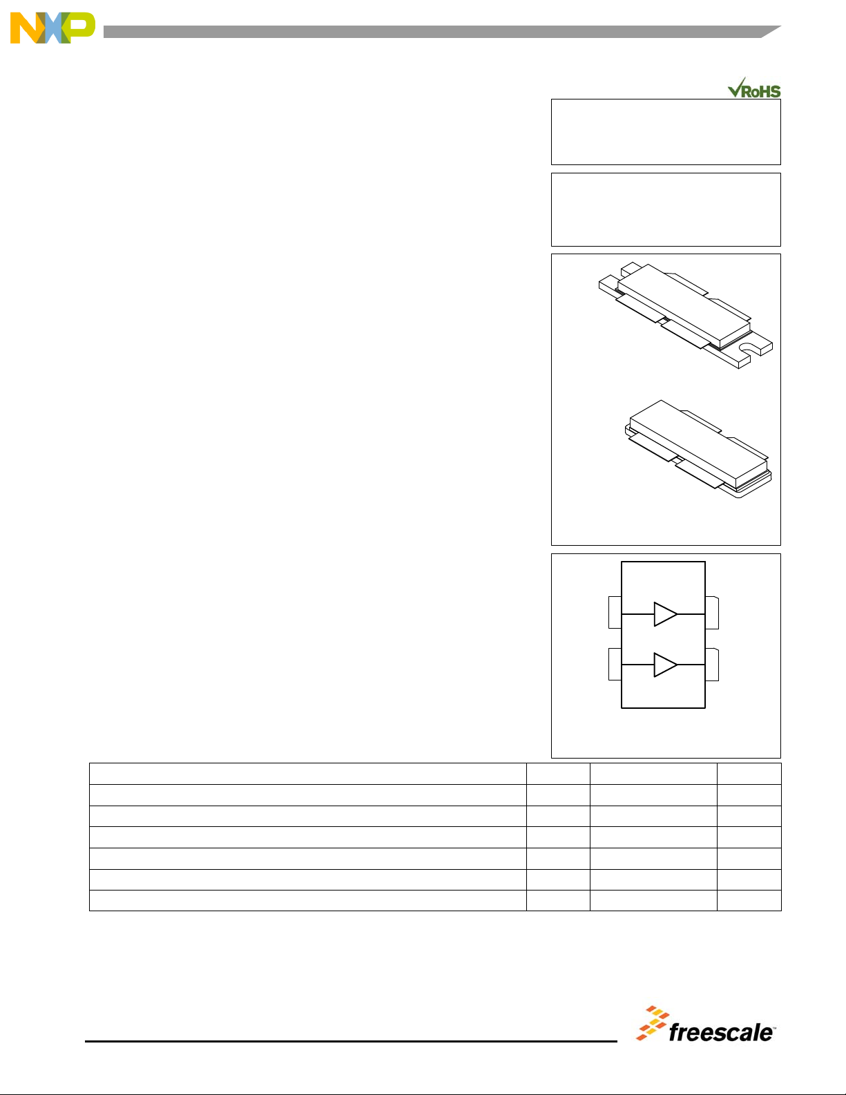
MMRF1006HR5
MMRF1006HSR5
10--500 MHz, 1000 W , 50 V
LATERAL N--CHANNEL
BROADBAND
RF POWER MOSFETs
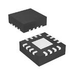
NI--1230H--4S
MMRF1006HR5
PARTS ARE PUSH--PULL
(Top View)
RF
outA
/V
DSA
31
42
RF
outB
/V
DSB
RF
inA
/V
GSA
RF
inB
/V
GSB
Figure 1. Pin Connections
NI--1230S--4S
MMRF1006HSR5
© Freescale Semiconductor, Inc., 2013, 2015.
A
ll rights reserved.
Verzeichnis