

herunterladen

Application Report
SNOA021C–May 2004–Revised May 2004
AN-1126 BGA (Ball Grid Array)
ABSTRACT
Leaders in the consumer electronics industry will be determined by their ability to deliver increasingly
miniaturized products at lower costs. The Ball Grid Array (BGA) package achieves these objectives by
providing increased functionality for the same package size while being compatible with existing Surface
Mount Technology (SMT) infrastructure.
Contents
1 Introduction .................................................................................................................. 3
2 Package Overview .......................................................................................................... 3
2.1 PBGA (PLASTIC BGA) CONSTRUCTION ..................................................................... 3
2.2 TE-PBGA (THERMALLY ENHANCED BGA) CONSTRUCTION ............................................ 4
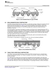
2.3 EBGA (ENHANCED BGA) CONSTRUCTION ................................................................. 5
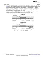
2.4 TSBGA (TAPE SUPER BGA) CONSTRUCTION .............................................................. 5
2.5 PACKAGE ELECTRICAL PERFORMANCE ................................................................... 7
3 Component Reliability ...................................................................................................... 7
4 Package Handling/Shipping Media ....................................................................................... 8
5 Design Recommendations ................................................................................................. 8
5.1 SOLDER PAD GEOMETRY ...................................................................................... 8
5.2 NSMD vs. SMD LAND PATTERN ............................................................................... 8
5.3 ESCAPE ROUTING GUIDELINES .............................................................................. 8
6 Assembly Recommendations ............................................................................................ 10
6.1 PROCESS FLOW & SET-UP RECOMMENDATION ........................................................ 10
6.2 PCB PLATING RECOMMENDATIONS ....................................................................... 11
6.3 SOLDER PASTE PRINTING .................................................................................... 11
6.4 PASTE RECOMMENDATIONS ................................................................................ 11
6.5 COMPONENT PLACEMENT ................................................................................... 11
6.6 REFLOW .......................................................................................................... 12
6.7 SOLDER JOINT INSPECTION ................................................................................. 13
6.8 REPLACEMENT AND REWORK .............................................................................. 14
6.9 SITE PREPARATION ............................................................................................ 14
6.10 COMPONENT PLACEMENT ................................................................................... 14
6.11 COMPONENT REFLOW ........................................................................................ 14
List of Figures
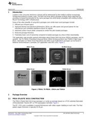
1 PBGA, TE-PBGA , EBGA and TSBGA .................................................................................. 3
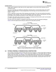
2 Cross-Sectional View of 2 and 4 Layer PBGA.......................................................................... 4
3 Cross-Sectional View of 4 Layer TE-PBGA ............................................................................. 5
4 Cross-Sectional View of EBGA ........................................................................................... 5
5 Cross-Sectional View of TSBGA Packages............................................................................. 6
6 Typical Process Flow....................................................................................................... 7
7 NSMD and SMD Pad Definition........................................................................................... 8
8 P = Pad Pitch D = Pad Diameter L = Line Width S = Line Space.................................................... 9
9 Routing for Four Rows of Solder Balls................................................................................... 9
10 Routing for Five Rows of Solder Balls.................................................................................. 10
All trademarks are the property of their respective owners.
1
SNOA021C–May 2004–Revised May 2004 AN-126 BGA (Ball Grid Array)
Submit Documentation Feedback
Copyright © 2004, Texas Instruments Incorporated