
herunterladen
10-Bit, 4× Oversampling
SDTV Video Decoder
Data Sheet
ADV7180
Rev. J Document Feedback
Information furnished by Analog Devices is believed to be accurate and reliable. However, no
responsibility is assumed by Analog Devices for its use, nor for any infringements of patents or other
rights of third parties that may result from its use. Specifications subject to change without notice. No
license is granted by implication or otherwise under any patent or patent rights of Analog Devices.
Trademarks and registered trademarks are the property of their respective owners.
One Technology Way, P.O. Box 9106, Norwood, MA 02062-9106, U.S.A.
Tel: 781.329.4700 ©2006-2015 Analog Devices, Inc. All rights reserved.
Technical Support www.analog.com
17BFEATURES
Qualified for automotive applications
Worldwide NTSC/PAL/SECAM color demodulation support
One 10-bit ADC, 4× oversampling for CVBS, 2× oversampling
for Y/C mode, and 2× oversampling for YPrPb (per channel)
3 video input channels with on-chip antialiasing filter
CVBS (composite), Y/C (S-Video), and YPrPb (component)
video input support
5-line adaptive comb filters and CTI/DNR video
enhancement
Mini-TBC functionality provided by adaptive digital line
length tracking (ADLLT), signal processing, and enhanced
FIFO management
Integrated AGC with adaptive peak white mode
Macrovision copy protection detection
NTSC/PAL/SECAM autodetection
8-bit ITU-R BT.656 YCrCb 4:2:2 output and HS, VS, and FIELD
1
1.0 V analog input signal range
Full-featured VBI data slicer with teletext support (WST)
Power-down mode and ultralow sleep mode current
2-wire serial MPU interface (I
2
C compatible)
Single 1.8 V supply possible
1.8 V analog, 1.8 V PLL, 1.8 V digital, 1.8 V to 3.3 V I/O supply
−10°C to +70°C commercial temperature grade
−40°C to +85°C industrial/automotive qualified temperature
grade
−40°C to +125°C temperature grade for automotive qualified
4 package types
64-lead, 10 mm × 10 mm, RoHS compliant LQFP
48-Lead, 7 mm × 7 mm, RoHS compliant LQFP
40-lead, 6 mm × 6 mm, RoHS compliant LFCSP
32-lead, 5 mm × 5 mm, RoHS compliant LFCSP
18BGENERAL DESCRIPTION
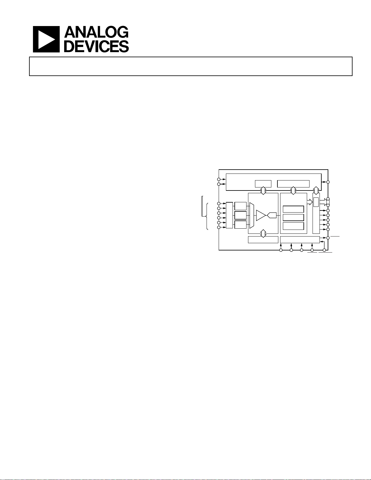
The ADV7180 automatically detects and converts standard
analog baseband television signals compatible with worldwide
NTSC, PAL, and SECAM standards into 4:2:2 component video
data compatible with the 8-bit ITU-R BT.656 interface standard.
The simple digital output interface connects gluelessly to a wide
range of MPEG encoders, codecs, mobile video processors, and
Analog Devices, Inc., digital video encoders, such as the ADV7391.
External HS, VS, and FIELD signals provide timing references
for LCD controllers and other video ASICs, if required. Accurate
10-bit analog-to-digital conversion provides professional quality
19BAPPLICATIONS
Digital camcorders and PDAs
Low cost SDTV PIP decoders for digital TVs
Multichannel DVRs for video security
AV receivers and video transcoding
PCI-/USB-based video capture and TV tuner cards
Personal media players and recorders
Smartphone/multimedia handsets
In-car/automotive infotainment units
Rearview camera/vehicle safety systems
20BFUNCTIONAL BLOCK DIAGRAM
0
5700-001
A
IN
1
A
IN
2
XTAL1
XTAL
A
IN
3
A
IN
4
1
A
IN
5
1
A
IN
6
1
ANALOG
VIDEO
INPUTS
AA
FILTER
AA
FILTER
AA
FILTER
DIGITAL
PROCESSING
BLOCK
2D COMB
VBI SLICER
COLOR
DEMOD
SCLK SDATA ALSB RESET PWRDWN
4
1
ONLY AVAILABLE ON 64-LEAD PACKAGE AND 48-LEAD PACKAGES.
2
16-BIT ONLY AVAILABLE ON 64-LEAD PACKAGE.
3
48-LEAD, 40-LEAD, AND 32-LEAD PACKAGE USES ONE LEAD FOR VS/FIELD.
4
NOT AVAILABLE ON 32-LEAD PACKAGE.
5
ONLY AVAILABLE ON 48-LEAD AND 64-LEAD PACKAGES.
10-BIT, 86MHz
ADC
REFERENCE
PLL ADLLT PROCESSING
CLOCK PROCESSING BLOCK
I
2
C/CONTROL
MUX BLOCK
FIFOOUTPUT BLOCK
ADV7180
SHA A/D
VS
LLC
HS
SFL
INTRQ
P15 TO P0
8-BIT/16-BIT
2
PIXEL DATA
FIELD
3
GPO
5
Figure 1.
video performance for consumer applications with true 8-bit
data resolution. Three analog video input channels accept standard
composite, S-Video, or component video signals, supporting a
wide range of consumer video sources. AGC and clamp-restore
circuitry allow an input video signal peak-to-peak range to 1.0 V.
Alternatively, these can be bypassed for manual settings.
The line-locked clock output allows the output data rate, timing
signals, and output clock signals to be synchronous, asynchronous,
or line locked even with ±5% line length variation. Output
control signals allow glueless interface connections in many
applications. The ADV7180 is programmed via a 2-wire, serial
bidirectional port (I
2
C-compatible) and is fabricated in a 1.8 V
CMOS process. Its monolithic CMOS construction ensures greater
functionality with lower power dissipation. LFCSP package options
make the decoder ideal for space-constrained portable applications.
The 64-lead LQFP package is pin compatible with the ADV7181C.
1
The 48-Lead LQFP, 40-lead LFCSP, and 32-lead LFCSP use one pin to output
VS or FIELD.
Verzeichnis
- ・ Konfiguration des Pinbelegungsdiagramms on Seite 14 Seite 15 Seite 16 Seite 18 Seite 20
- ・ Abmessungen des Paketumrisses on Seite 113
- ・ Paket-Footprint-Pad-Layout on Seite 108
- ・ Teilenummerierungssystem on Seite 115
- ・ Blockdiagramm on Seite 1 Seite 7 Seite 8 Seite 27 Seite 42
- ・ Typisches Anwendungsschaltbild on Seite 7 Seite 109 Seite 110 Seite 111 Seite 112
- ・ Schweißen Temperatur on Seite 13
- ・ Beschreibung der Funktionen on Seite 1 Seite 14 Seite 15 Seite 16 Seite 18
- ・ Technische Daten on Seite 1 Seite 9 Seite 10 Seite 11 Seite 12
- ・ Anwendungsbereich on Seite 1 Seite 115
- ・ Elektrische Spezifikation on Seite 9