
herunterladen
1
®
©
1997 Burr-Brown Corporation AB-122 Printed in U.S.A. September, 1997
INTERFACING THE ADS7822 TO THE SYNCHRONOUS
SERIAL PORT OF THE 80x51 MICROCONTROLLER
By Gebhard Haug and Bonnie C. Baker
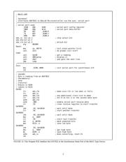
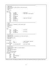
Analog-to-digital converters can be controlled by a normal
I/O port or with the synchronous serial port of the 80x51
microcontrollers. The synchronous serial port is more effi-
cient, however, there are some pitfalls to be aware of when
configuring the 8-pin A/D converters (ADS1286, ADS7816,
ADS7817 and ADS7822) from Burr-Brown. This applica-
tion bulletin describes how to get around these pitfalls and
get the best performance out of this combination.
The ADS1286, ADS7816, ADS7817, and ADS7822 are all
12-bit converters that are available in a variety of 8-pin
packages. These devices are classical successive approxi-
mation register (SAR) A/D converters. Their architecture is
based on capacitive redistribution, which inherently in-
cludes a sample/hold function. All four of these converters
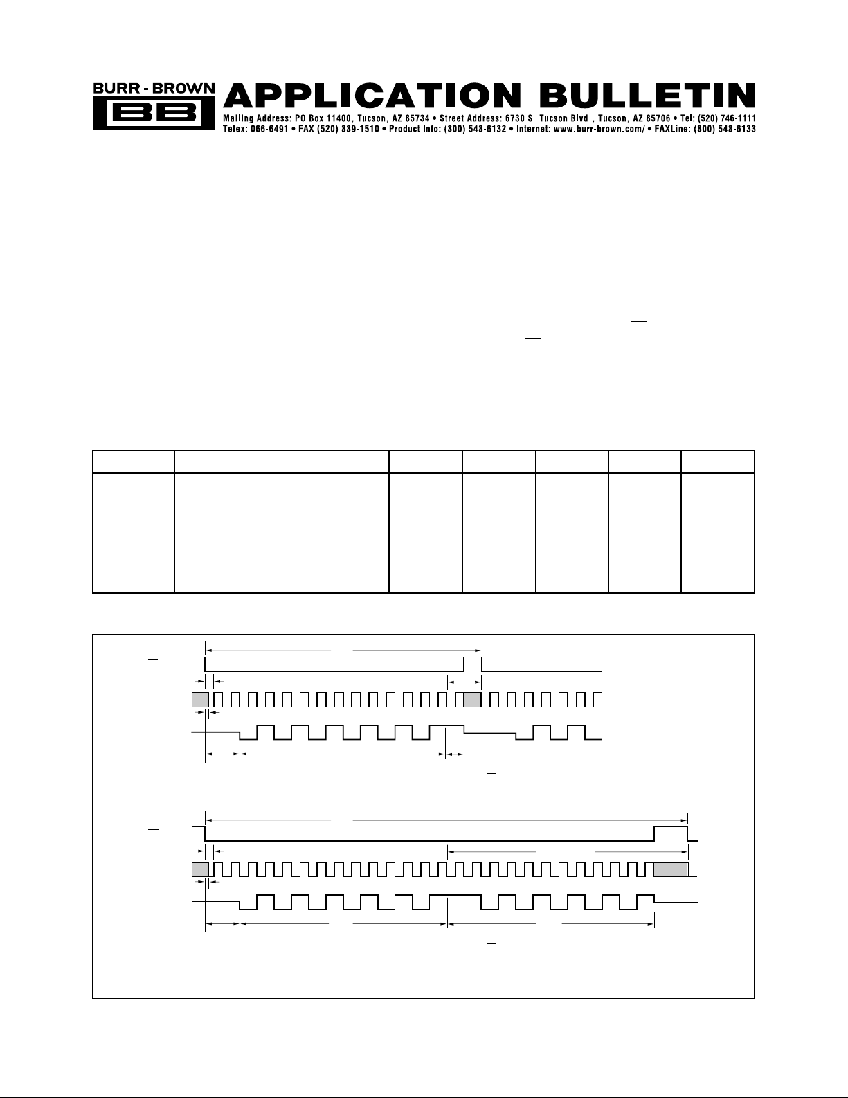
have three digital communication lines in their interface.
These communication lines are CS/SHDN, D
OUT
and
DCLOCK. The CS/SHDN pin provides a chip select func-
tion when LOW. When this pin is pulled HIGH, the A/D
converter goes into its shutdown mode. The basic timing
diagram for these A/D converters is shown in Figure 1. The
timing specifications for the individual A/D converters are
called out in Table 1.
SYMBOL DESCRIPTION ADS1286 ADS7816 ADS7817 ADS7822 UNITS
t
SMPL
Analog Input Sample Time 1.5 (typ) 1.5 (min) 1.5 (min) 1.5 (min) Clk Cycles
2.0 (max) 2.0 (max) 2.0 (max)
t
CONV
Conversion Time 12 12 12 12 Clk Cycles
t
CYC
Throughput Rate 20 (max) 200 (max) 200 (max) 75 (max) kHz
t
CSD
CS Falling to DCLOCK LOW 0 (max) 0 (max) 0 (max) 0 (max) ns
t
SUCS
CS Falling to DCLOCK Rising 30 (min) 30 (min) 30 (min) 30 (min) ns
t
hDO
DCLOCK Falling to Current D
OUT
not Valid 15 (min) 15 (min) 15 (min) 15 (min) ns
t
dDO
DCLOCK Falling to Next D
OUT
Valid 150 (max) 150 (max) 150 (max) 200 (max) ns
TABLE I. Timing Specifications for the ADS1286, ADS7816, ADS7817, and ADS7822.
CS/SHDN
D
OUT
DCLOCK
t
DATA
t
SUCS
t
CSD
t
CYC
t
CONV
POWER
DOWN
t
SMPL
Note: (1) After completing the data transfer, if further clocks are applied with CS
LOW, the ADC will output LSB-First data then followed with zeroes indefinitely.
B11
(MSB)
B10 B9 B8 B7 B6 B5 B4 B3 B2 B1 B0
(1)
NULL
BIT
HI-ZHI-Z
B11 B10 B9 B8
NULL
BIT
CS/SHDN
D
OUT
DCLOCK
t
CONV
t
DATA
t
SUCS
t
CYC
POWER DOWN
t
SMPL
Note: (2) After completing the data transfer, if further clocks are applied with CS
LOW, the ADC will output zeroes indefinitely.
t
DATA
: During this time, the bias current and the comparator power down and the reference input
becomes a high impedance node, leaving the CLK running to clock out LSB-First data or zeroes.
B11
(MSB)
B10 B9 B8 B7 B6 B5 B4 B4B3 B3B2 B2B1 B1B0
NULL
BIT
HI-Z HI-Z
B5 B6 B7 B8 B9 B10 B11
(2)
t
CSD
FIGURE 1. Timing Diagram for the ADS1286, ADS7816, ADS7817, and ADS7822.
SBAA018
Verzeichnis