
herunterladen
CDAC ARCHITECTURE PLUS RESISTOR DIVIDER GIVES ADC574
PINOUT WITH SAMPLING, LOW POWER, NEW INPUT RANGES
George Hill (602) 746-7283
Modern successive-approximation analog-to-digital converter
ICs are replacing older current-mode D/A structures with
capacitor arrays, called CDACs (for Capacitor D/A). This
change makes it easier to combine the analog components of
the converter with the digital elements in standard CMOS
structures. Additionally, the capacitor input structure adds
inherent sampling to the A/D, at a time when more and more
A/D applications are involved in signal processing.
This application note compares basic current-mode succes-
sive approximation A/Ds with CDAC-based architectures,
and shows how adding a resistor divider network to the
CDAC input permits the Burr-Brown ADS574 and ADS774
to fit existing ADC574 sockets. It then goes on to describe
some new analog input voltage ranges available on these
parts due to the resistor network and CDAC approach.
The ADS574 and ADS774 plug into ADC574/674/774 sock-
ets and handle all of their standard input ranges (0V to 10V,
±5V, ±10V, and 0V to 20V), as discussed in their full data
sheets. They can operate from standard ±15V and +5V
supplies, or from a single +5V supply. The input divider
structure makes it possible to take advantage of this +5V
supply operation to build complete data acquisition systems
that run from a single +5V supply, with several different
input ranges pin-selectable.
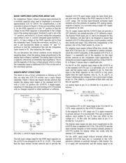
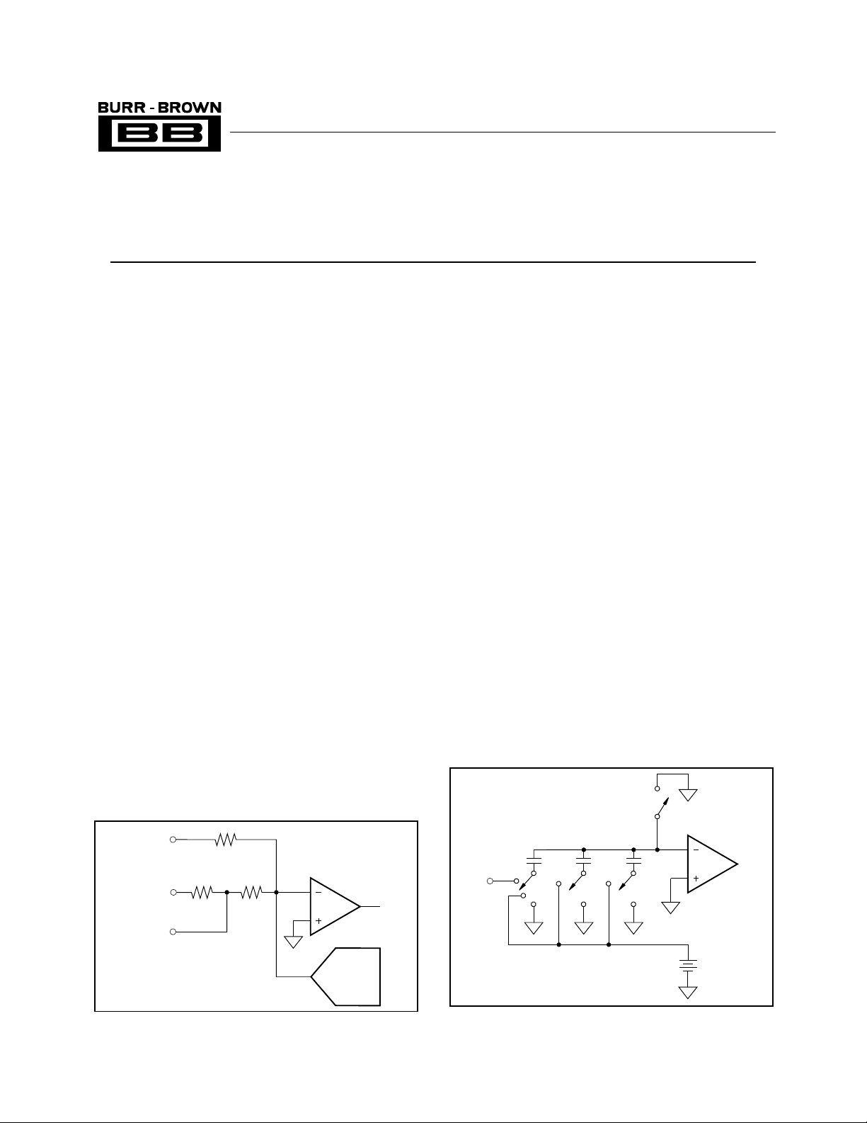
TRADITIONAL ADC574 INPUT STRUCTURE
Let’s start by taking a look at the input ranges on the
traditional ADC574, the most widely used 12-bit A/D in the
world. Figure 1 shows the standard input divider network
and comparator/current D/A structure used to implement the
front end of this successive approximation A/D.
These three pins allow the selection of four different analog
input ranges: 0V to +10V, 0V to +20V, ±5V, and ±10V. The
simplicity of this circuit takes advantage of the virtual
ground at the negative input to the comparator at the end of
the successive approximation process, when the negative
input to the comparator is very close to 0V.
The internal current D/A in the ADC574 has a unipolar
output of 0mA to –2mA, so that it can balance out the 0mA
to 2mA generated by full scale analog inputs (20V across
10kΩ or 10V across 5kΩ.) By grounding pin 12, a unipolar
0V to 20V input range is achieved by driving pin 14 and
leaving pin 13 unconnected. Reversing pins 13 and 14 sets
up the ADC574 for a 0V to 10V input range.
Connecting pin 12 to the 10V, reference provided on an
ADC574 injects an offset that allows pins 13 or 14 to handle
bipolar input ranges of ±5V or ±10V, respectively. The
current injected by the reference at pin 12 adds to the input
current generated by the analog input signal to insure that the
unipolar current flow from the internal current D/A need
only be unipolar.
During conversion, the analog signal conditioning in a
system must hold the input stable (using a sample/hold
amplifier or processing slow signals such as thermocouples.)
The successive approximation logic tests the current D/A in
various settings until the current sinked into the D/A bal-
ances the current generated by the analog input signal (plus
the current from the Bipolar Offset resistor in bipolar ranges)
to within ±1/2 LSB.
APPLICATION BULLETIN
®
Mailing Address: PO Box 11400 • Tucson, AZ 85734 • Street Address: 6730 S. Tucson Blvd. • Tucson, AZ 85706
Tel: (602) 746-1111 • Twx: 910-952-111 • Telex: 066-6491 • FAX (602) 889-1510 • Immediate Product Info: (800) 548-6132
R
1
10kΩ
5kΩ
R
3
Pin 14
Pin 12
20V Range
Bipolar Offset
5kΩ
R
2
Pin 13
10V Range
12-Bit
0 to –2mA
D/A
Converter
Comparator
FIGURE 1. Traditional ADC574 Input Structure.
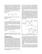
FIGURE 2. Simplified 3-bit Switched Capacitor Array A/D.
Comparator
R
G
R
G
S
1
S
2
S
3
C2C4C
S
Analog
Input
+
Reference
S
C
RG
©
1991 Burr-Brown Corporation AN-178 Printed in U.S.A. September, 1991
SBAA043