
herunterladen
AN-934
APPLICATION NOTE
One Technology Way • P. O. Box 9106 • Norwood, MA 02062-9106, U.S.A. • Te l: 781.329.4700 • Fax: 781.461.3113 • www.analog.com
60 dB Wide Dynamic Range, Low Frequency AGC Circuit Using a Single VGA
by James Staley
Rev. 0 | Page 1 of 4
INTRODUCTION
Low frequency automatic gain control (AGC) circuits are used
in audio and power equipment for applications such as sensitive
microphone preamplifiers (preamps) and regulators. An AGC
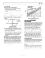
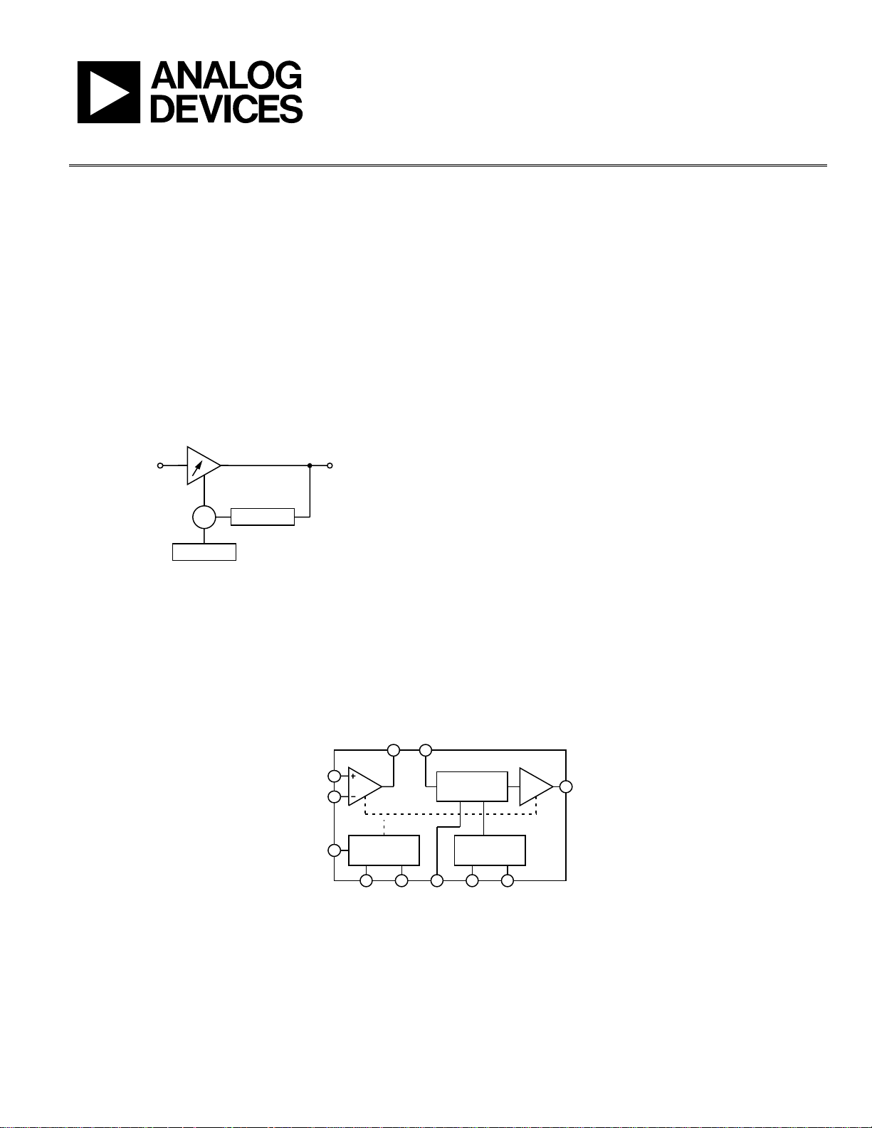
circuit, a closed-loop feedback system, is shown in
Figure 1. The
loop consists of a controllable gain element, a detector, a stable
reference and a comparison circuit.
06975-001
INPUT OUTPU
T
CONTROLLABLE
GAIN
ELEMENT
GAIN CONTROL
VOLTAGE
+
–
REFERENCE
DETECTOR
Figure 1. AGC Circuit Using a Variable Gain Amplifier
This application note describes a low frequency AGC circuit
using a wide dynamic range AD8336 variable gain amplifier
(VGA) as the gain control element, an AD736 rms-to-dc
converter as the detector, a low cost rail-to-rail AD8551 op amp,
and an ADP3339 LDO as the reference. Because of its wide
controllable gain range and circuit flexibility, the AD8336 is
featured in this application note.
Controllable Gain Element
A VGA is a special type of amplifier, which controls its gain by
electronic means instead of by a set of fixed resistors, as is the
case with the classic op amp circuit. VGAs are the familiar and
preferred solution for automatic gain control circuits in a
variety of communications applications.
VGAs operate at frequencies from hundreds of kilohertz up to
hundreds of megahertz. An ideal VGA performs as a linear
amplifier, without introducing distortion or otherwise
corrupting the desired signal.
When a VGA is used, the gain element is an amplifier combined
with electronic volume control. In this example, the controllable
gain element is further reduced to an electronic potentiometer
and a fixed gain amplifier and it adjusts the loop gain by
attenuating the input signal, without contributing significant
distortion. The other fundamental elements of the loop are the
detector, a stable reference, and a summing circuit that senses
the state of the loop, compares it to the stable reference, and
adjusts the output accordingly.
A functional block diagram of the AD8336 is shown in
Figure 2.
0
6975-002
4
1
8
5
9
PrA
AD8336
PRAO
VNEG VPOS VCOM GPOS GNEG
V
GAI
ATTENUATOR
–60dB TO 0dB
BIAS
GAIN CONTROL
INTERFACE
2
10 13 3 11 12
34dB
V
OUT
INPP
INPN
PWRA
Figure 2. AD8336 Functional Block Diagram