
herunterladen
AN-873
APPLICATION NOTE
One Technology Way • P. O. Box 9106 • Norwood, MA 02062-9106, U.S.A. • Tel : 781.329.4700 • Fax: 781.461.3113 • www.analog.com
Lock Detect on the ADF4xxx Family of PLL Synthesizers
by Peadar Forbes and Ian Collins
Rev. 0 | Page 1 of 8
INTRODUCTION
This application note covers the ADF4xxx family of integer-N
PLL synthesizers and the ADF4360-x family of integrated phase
locked loop (PLL) synthesizers and voltage controlled oscillators
(VCO). (See the
Appendix for a full list of the ADF4xxx parts
covered in the AN-873 application note.) There are two forms
of lock detect available on each part: analog lock detect (ALD)
and digital lock detect (DLD). Each has its advantages and
disadvantages, depending on the application. The aim of this
application note is to explain both options and allow the user to
make an informed decision as to which form of lock detect to use.
Both ALD and DLD use the phase error at the phase frequency
detector (PFD) inputs to decide whether the PLL is in lock.
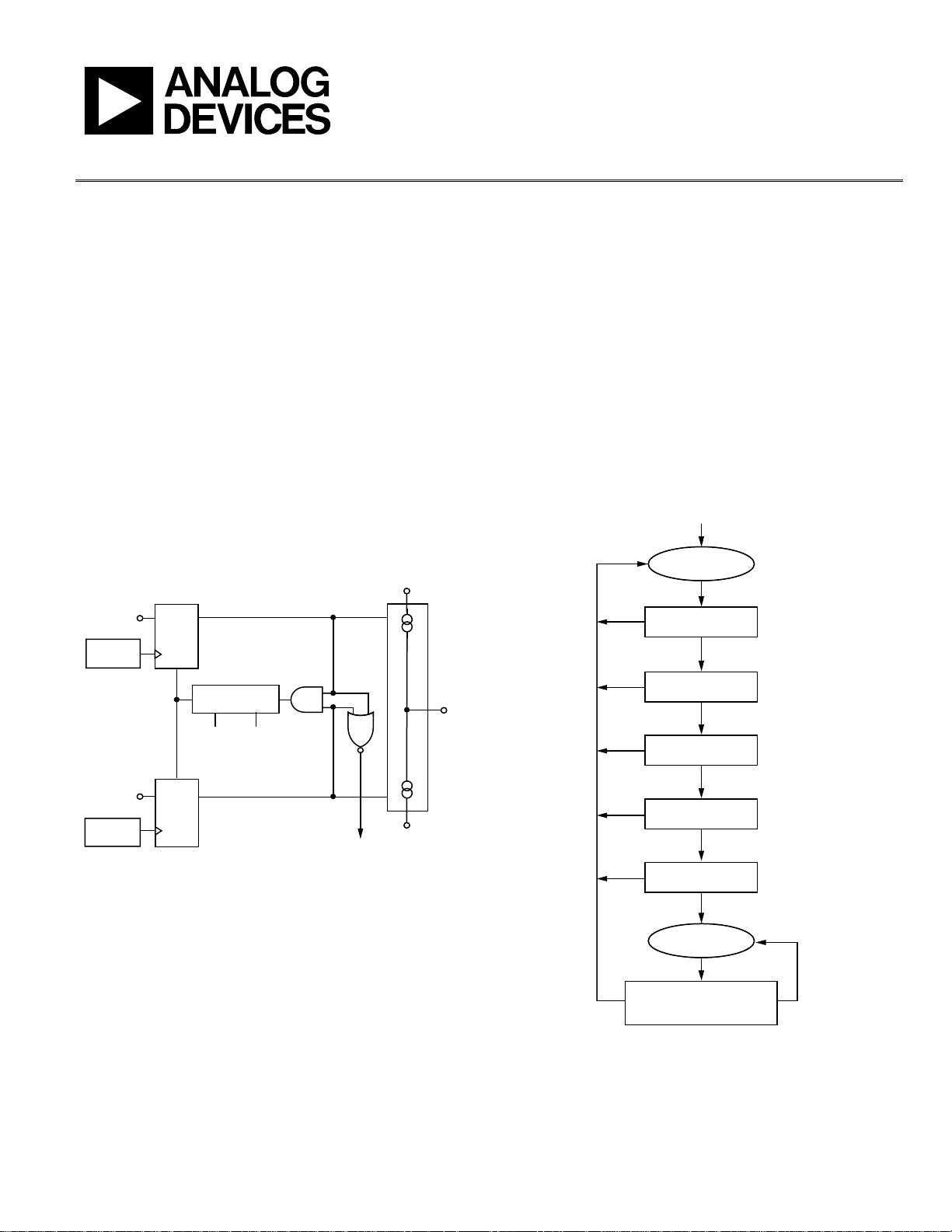
Figure 1 shows the PFD and charge pump block.
HI
HI
D1
D2
Q1
Q2
CLR2
CP
U1
U2
UP
DOWN
ABP2
ABP1
U3
R DIVIDER
PROGRAMMABLE
DELAY
N DIVIDER
V
P
CHARGE
PUMP
CLR1
ANALOG LOCK
DETECT
(OPEN DRAIN OUTPUT)
CPGND
06391-001
Figure 1. PFD and Charge Pump on the ADF4xxx Family of PLL Synthesizers
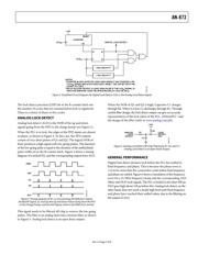
DIGITAL LOCK DETECT
Digital lock detect outputs either a CMOS logic high, indicating
a locked PLL state, or a logic low, indicating an unlocked state.
The state diagram for DLD is shown in
Figure 2, and a simplified
circuit diagram is shown in
Figure 3. It works by measuring the
phase error at the PFD inputs and using a window of 15 ns
phase error to decide the lock status of the PLL.
When the phase error at the PFD inputs on five or more consecu-
tive cycles is inside the 15 ns window, it considers the PLL to be
in lock and outputs a logic high.
When the phase error drifts outside of the loss of lock threshold
(30 ns) on any subsequent PFD cycle, it registers an out-of-lock
condition, that is, a logic low. In some of the PLL parts, the
windows are set by the R
SET
resistor (see the Digital Lock
Detect—Dependence on R
SET
section). The 15 ns window
and the 30 ns window are for an R
SET
resistor of 4.7 k.
DLD = 0
PFD PHASE ERROR
< DLD WINDOW (15ns)
PFD PHASE ERROR
< DLD WINDOW (15ns)
PFD PHASE ERROR
< DLD WINDOW (15ns)
PFD PHASE ERROR
< DLD WINDOW (15ns)
PFD PHASE ERROR
< DLD WINDOW (15ns)
DLD = 1
YES
YES
YES
YES
YES
PFD PHASE ERROR
> LOSS OF LOCK
THRESHOLD (30ns)
YES NO
NO
NO
NO
NO
NO
START
06391-002
Figure 2. State Diagram for Digital Lock Detect
(Lock Detect Precision (LDP) is 5 in This Case)