

herunterladen
AN-0983
APPLICATION NOTE
One Technology Way • P. O. Box 9106 • Norwood, MA 02062-9106, U.S.A. • Te l: 781.329.4700 • Fax: 781.461.3113 • www.analog.com
Introduction to Zero-Delay Clock Timing Techniques
by Ken Gentile
Rev. 0 | Page 1 of 8
Zero-delay refers to the ability of a clock synthesizer to provide
an output signal that is edge aligned with a clock reference
source. Applications include many synchronous systems, such
as the SONET and SDH networks, high speed network servers,
network line cards, as well as baseband timing for W-CDMA
and Wi-Fi.
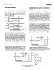
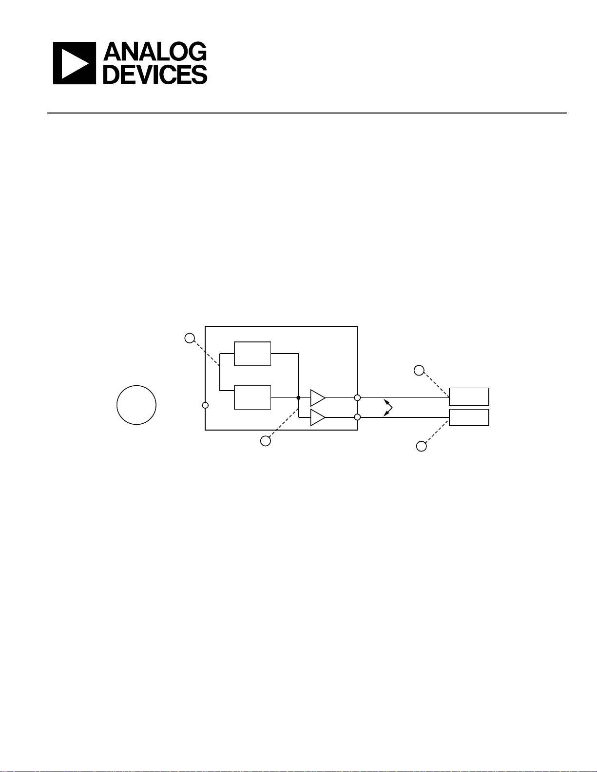
ZERO-DELAY ARCHITECTURE
At a minimum, an integrated zero-delay clock synthesizer
requires three building blocks (see Figure 1). The first building
block is a phase-locked loop (PLL), of either the common
analog variety or one of the more recent all-digital designs.
The second building block is two (or more) output drivers with
matched propagation delay. The third building block is a varia-
ble delay element in the feedback path of the PLL. In addition,
the zero-delay architecture requires equal interconnect delay
from the synthesizer outputs to their associated target devices.
Equal interconnect delay is a fundamental component of the
zero-delay architecture. Without it, clock edge alignment at the
target devices is not possible.
07845-001
OUTPUT DRIVERS
WITH MATCHED
PROPAGATION
DELAY
CLOCK
SOURCE
OUT
A
REF
A
C
B
D
ZERO-DELAY CLOCK SYNTHESIZER
TARGET
DEVICE B
TARGET
DEVICE A
EQUAL
INTERCONNECT
DELAY
OUT
B
VARIABLE
DELAY
ELEMENT
PLL
Figure 1. Generic Zero-Delay Synthesizer
Verzeichnis
- ・ Blockdiagramm on Seite 4
- ・ Anwendungsbereich on Seite 1