
herunterladen
REV. A
a
Information furnished by Analog Devices is believed to be accurate and
reliable. However, no responsibility is assumed by Analog Devices for its
use, nor for any infringements of patents or other rights of third parties that
may result from its use. No license is granted by implication or otherwise
under any patent or patent rights of Analog Devices.
One Technology Way, P.O. Box 9106, Norwood, MA 02062-9106, U.S.A.
Tel: 781/329-4700 www.analog.com
Fax: 781/326-8703 © Analog Devices, Inc., 2002
AD8304
160 dB Range (100 pA –10 mA)
Logarithmic Converter
FEATURES
Optimized for Fiber Optic Photodiode Interfacing
Eight Full Decades of Range
Law Conformance 0.1 dB from 1 nA to 1 mA
Single-Supply Operation (3.0 V– 5.5 V)
Complete and Temperature Stable
Accurate Laser-Trimmed Scaling:
Logarithmic Slope of 10 mV/dB (at VLOG Pin)
Basic Logarithmic Intercept at 100 pA
Easy Adjustment of Slope and Intercept
Output Bandwidth of 10 MHz, 15 V/s Slew Rate
1-, 2-, or 3-Pole Low-Pass Filtering at Output
Miniature 14-Lead Package (TSSOP)
Low Power: ~4.5 mA Quiescent Current (Enabled)
APPLICATIONS
High Accuracy Optical Power Measurement
Wide Range Baseband Log Compression
Versatile Detector for APC Loops
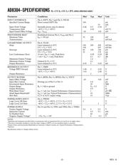
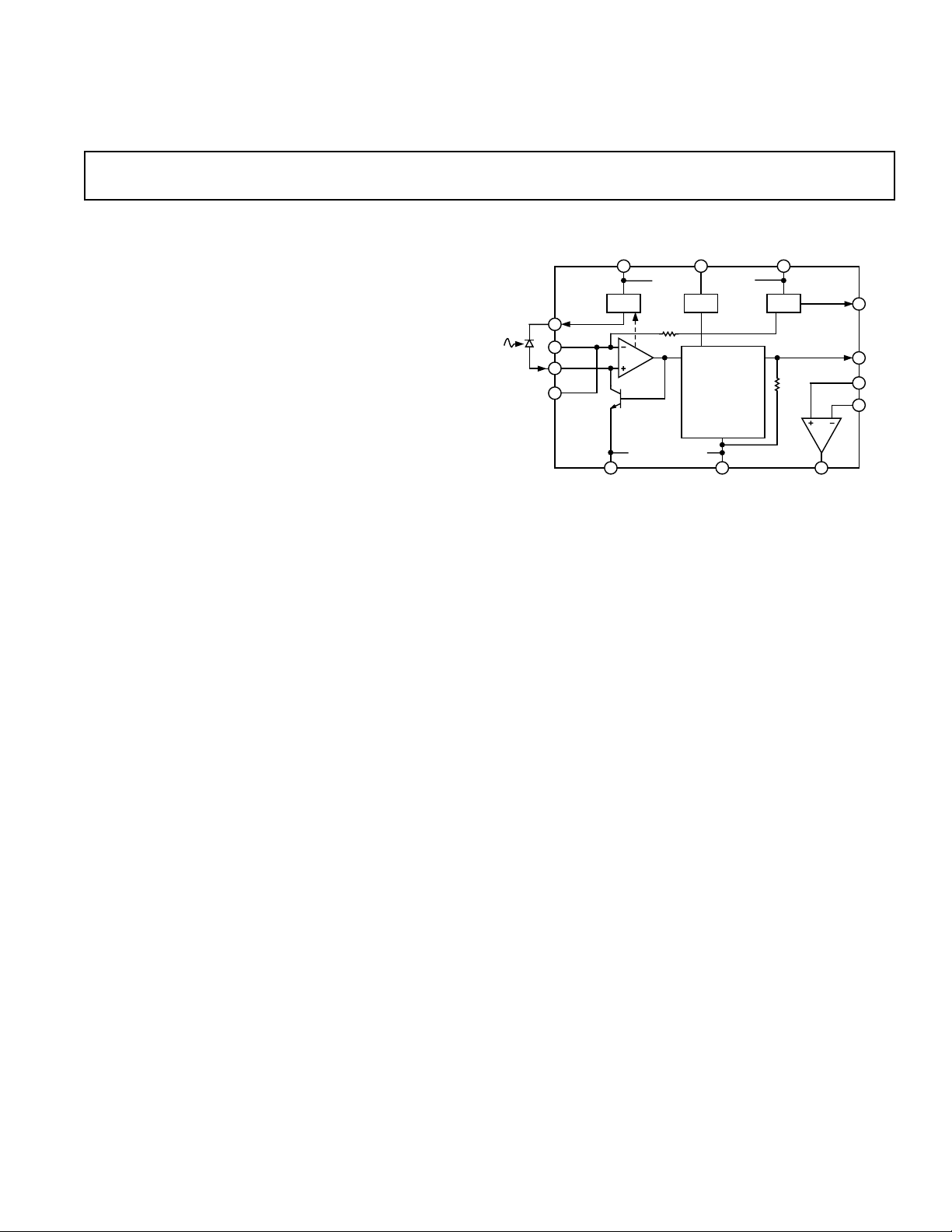
FUNCTIONAL BLOCK DIAGRAM
6
3
4
PDB BIAS VREF
10
2 12
I
PD
VPDB
VSUM
INPT
VSUM
5
1
VNEG
~10k
ACOM
14
VPS2 PWDN VPS1
VREF
7
VLOG
8
BFIN
9
BFNG
13
TEMPERATURE
COMPENSATION
5k
11
VOUT
0.5V
AD8304
PRODUCT DESCRIPTION
The AD8304 is a monolithic logarithmic detector optimized for
the measurement of low frequency signal power in fiber optic
systems. It uses an advanced translinear technique to provide an
exceptionally large dynamic range in a versatile and easily used
form. Its wide measurement range and accuracy are achieved
using proprietary design techniques and precise laser trimming.
In most applications only a single positive supply, V
P
, of 5 V
will be required, but 3.0 V to 5.5 V can be used, and certain
applications benefit from the added use of a negative supply,
V
N
. When using low supply voltages, the log slope is readily
altered to fit the available span. The low quiescent current and
chip disable features facilitate use in battery-operated applications.
The input current, I
PD
, flows in the collector of an optimally
scaled NPN transistor, connected in a feedback path around a
low offset JFET amplifier. The current-summing input node
operates at a constant voltage, independent of current, with a
default value of 0.5 V; this may be adjusted over a wide range,
including ground or below, using an optional negative supply.
An adaptive biasing scheme is provided for reducing the dark
current at very low light input levels. The voltage at Pin VPDB
applies approximately 0.1 V across the diode for I
PD
= 100 pA,
rising linearly with current to 2.0 V of net bias at I
PD
= 10 mA.
The input pin INPT is flanked by the guard pins VSUM that
track the voltage at the summing node to minimize leakage.
The default value of the logarithmic slope at the output VLOG is
accurately scaled to 10 mV/dB (200 mV/decade). The resistance
at this output is laser-trimmed to 5 kΩ, allowing the slope to be
lowered by shunting it with an external resistance; the addition
of a capacitor at this pin provides a simple low-pass filter. The
intermediate voltage VLOG is buffered in an output stage that can
swing to within about 100 mV of ground (or V
N
) and the posi-
tive supply, V
P
, and provides a peak current drive capacity of
±20 mA. The slope can be increased using the buffer and a pair
of external feedback resistors. An accurate voltage reference of
2V is also provided to facilitate the repositioning of the intercept.
Many operational modes are possible. For example, low-pass filters
of up to three poles may be implemented, to reduce the output
noise at low input currents. The buffer may also serve as a com-
parator, with or without hysteresis, using the 2 V reference, for
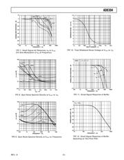
example, in alarm applications. The incremental bandwidth of
a translinear logarithmic amplifier inherently diminishes for small
input currents. At the 1 nA level, the AD8304’s bandwidth is
about 2 kHz, but this increases in proportion to I
PD
up to a
maximum value of 10 MHz.
The AD8304 is available in a 14-lead TSSOP package and specified
for operation from –40°C to +85°C.
Verzeichnis