
herunterladen
Circuit Note
CN-0056
Circuit Designs Using Analog Devices Products
Apply these product pairings quickly and with confidence.
For more information and/or support call 1-800-AnalogD
(1-800-262-5643) or visit www.analog.com/circuit.
Devices Connected/Referenced
ADL5315
Precision Wide-Range High-Side Current
Mirror
AD8304/
AD8305
Logarithmic Amplifier
ADL5306/
ADL5310
Single/Dual Logarithmic Amplifier
Interfacing the ADL5315 High Side Current Mirror to a Translinear Logarithmic
Amplifier in a Photodiode Power Detector Application
Rev. A
“Circuits from the Lab” from Analog Devices have been designed and built by Analog Devices
engineers. Standard engineering practices have been employed in the design and construction of
each circuit, and their function and performance have been tested and verified in a lab environment
at room temperature. However, you are solely responsible for testing the circuit and determining its
suitability and applicability for your use and application. Accordingly, in no event shall Analog
Devices be liable for direct, indirect, special, incidental, consequential or punitive damages due to
any cause whatsoever connected to the use of any “Circuit from the Lab”. (Continued on last page)
One Technology Way, P.O. Box 9106, Norwood, MA 02062-9106, U.S.A.
Tel: 781.329.4700
www.analog.com
Fax: 781.461.3113 ©2009-2010 Analog Devices, Inc. All rights reserved.
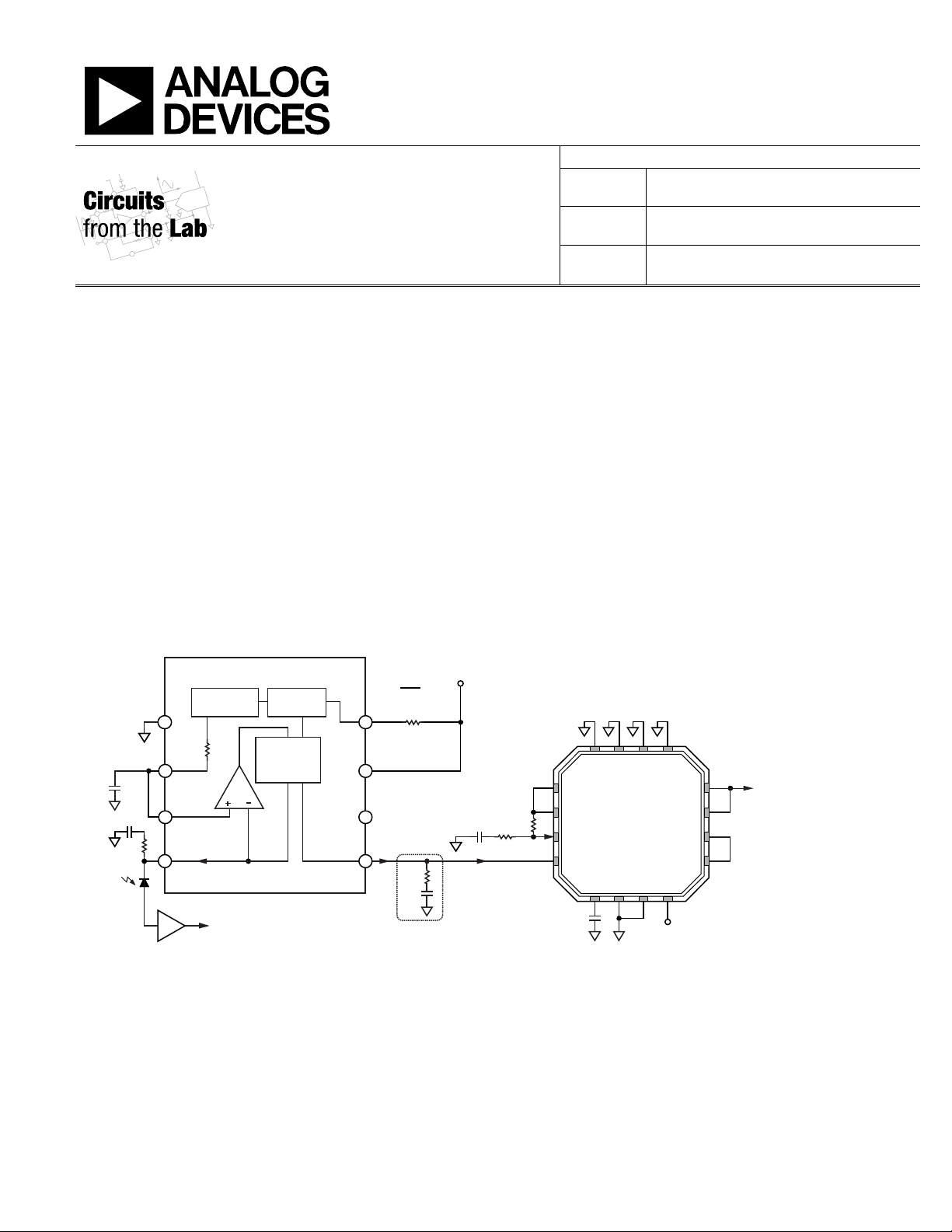
CIRCUIT FUNCTION AND BENEFITS
The ADL5315 addresses the need for precision high-side
monitoring of PIN photodiode current in fiber optic systems
and is useful in many nonoptical applications as well. It is
optimized for use with the Analog Devices, Inc., family of
translinear logarithmic amplifiers, which take advantage of the
wide input current range of the ADL5315. The circuit presented
in this document and shown in Figure 1 provides high accuracy
power monitoring using the ADL5315 precision wide-range,
high-side current mirror and the AD8305 translinear logarithmic
amplifier (log amp). This configuration is ideal for high
accuracy power monitoring because the full current mirror
range (3 nA to 3 mA) of the ADL5315 can be used.
The measured rms noise voltage at the output of the AD8305 vs.
the input current is shown in Figure 2, both for the AD8305 by
itself and in cascade with the ADL5315. The relatively low noise
produced by the ADL5315, combined with the additional noise
filtering inherent in the frequency response characteristics of
the AD8305, results in minimal degradation to the noise
performance of the AD8305.
08621-001
VOLTAGE
REFERENCE
CURRENT
LIMITING
COMM
VSET
NC
INPT
DATA PATH
AD8305 INPUT
COMPENSATION
NETWORK
I
PD
CURRENT
MIRROR
1:1
ADL5315
4
2 7
SREF
3
1
6
VPOS
PIN
20kΩ
5
RLIM
R
LIM
I
LIM
= 1mA – 16mA
3V TO 12V
8
IOUT
I
PD
TIA
1
2
3
4
11
SCAL
12
VOUT
10
BFIN
9
VLOG
5
VSUM
6
VNEG
7
VNEG
8
VPOS
15
COMM
16
COMM
14
COMM
13
COMM
AD8305
VRDZ
VREF
IREF
INPT
OUTPUT
V
OUT
= 0.2 × LOG
10
(I
PDM
/1nA)
200kΩ
2kΩ
4.7nF
1nF
1kΩ
0.1µF
C
SET
V
POS
R
LIM
= 48V
I
LIM
– 3kΩ
Figure 1. Connecting the ADL5315 to the AD8305 (Simplified Schematic: Decoupling and All Connections Not Shown)
Verzeichnis