
herunterladen
AN-931
APPLICATION NOTE
One Technology Way • P. O. Box 9106 • Norwood, MA 02062-9106, U.S.A. • Te l: 781.329.4700 • Fax: 781.461.3113 • www.analog.com
Understanding PulSAR ADC Support Circuitry
by Martin Murnane and Chris Augusta
Rev. 0 | Page 1 of 4
INTRODUCTION
Successive approximation register (SAR) analog-to-digital
converters (ADCs) use various new techniques for improved
resolution. Understanding how these devices work is important
in preventing malfunction and erroneous issues. This applica-
tion note discusses in general the pitfalls that occur regularly
when using SAR ADCs and, more importantly, how to easily
prevent them.
HOW DO PulSARs WORK?
The Analog Devices, Inc., PulSAR® family of ADCs uses inter-
nal switched capacitor techniques to extend the resolution of
SAR ADCs to 18 bits. This means that on a CMOS process, the
need for expensive thin film laser trimming is not required.
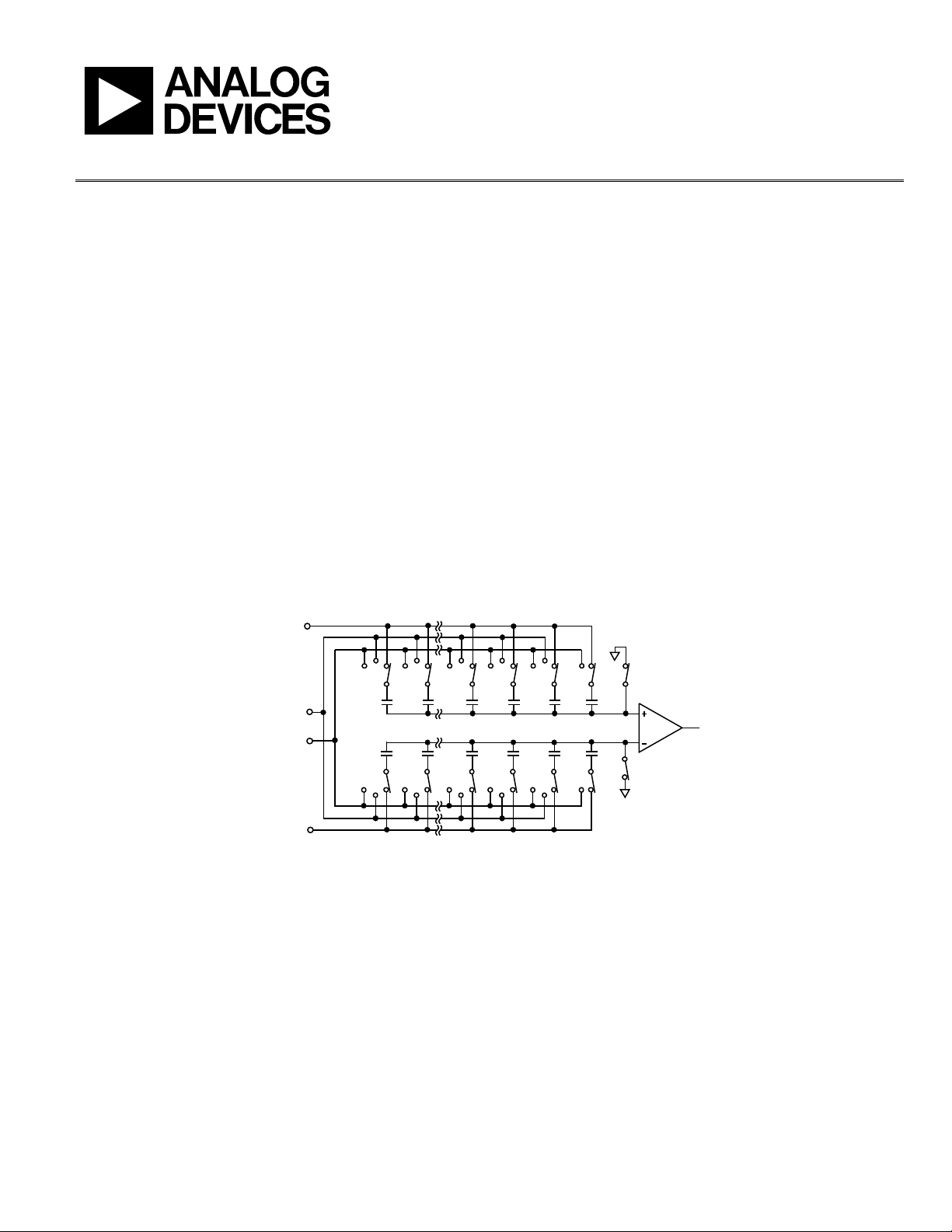
A simplified input stage of the AD7643 is shown in Figure 1.
The AD7643, an 18-bit ADC, capable of converting 1.25 MSPS,
is based on a charge-redistribution digital-to-analog converter
(DAC), which is popular in the newer SAR ADCs. The SAR
algorithm takes two phases to determine the ADC output code.
The first phase is the acquisition phase, where the SW+ and
SW− are initially closed. All switches are connected to the IN+
and IN− analog inputs, thus each capacitor is used as a sampling
capacitor acquiring the analog signal at the input. The second
phase is the conversion phase where the SW+ and SW− are
open. The inputs are disconnected from the internal capacitors
and applied to the comparator inputs. This results in an unstable
comparator. Without detailing the SAR algorithm, switching
each element of the array between REF and REFGND starting
with the MSB, brings the comparator back into a balanced
condition and thus generates the output code representing
the analog input signal.
SW+
COMP
SW–
IN+
REF
REFGND
LSB
MSB
131,072C
65,536C 4C 2C C C
IN–
4C 2C C C
LSB
MSB
AGND
AGND
131,072C
65,536C
06943-001
Figure 1. AD7643 Simplified Schematic
Verzeichnis
- ・ Blockdiagramm on Seite 1
- ・ Technische Daten on Seite 2 Seite 4