
herunterladen
AN-912
APPLICATION NOTE
One Technology Way • P. O. Box 9106 • Norwood, MA 02062-9106, U.S.A. • Te l: 781.329.4700 • Fax: 781.461.3113 • www.analog.com
Driving a Center-Tapped Transformer with a Balanced Current-Output DAC
by Ken Gentile
Rev. 0 | Page 1 of 12
The use of a center-tapped transformer as the output interface
for a balanced current-output DAC offers several benefits.
First, transformer coupling offers dc isolation between the
DAC output and the final load. It can also aid in the rejection
of common-mode signals present at the DAC output. Further-
more, transformer coupling can mitigate the even harmonics
that result from an imbalance between the DAC outputs.
Finally, all transformers have a limited bandwidth, which can
be used to advantage for suppressing the Nyquist images that
typically appear in a DAC output spectrum.
The goal of this application note is two-fold. The first goal is to
provide an explanation of the functionality of a balanced output
in the context of a current-output DAC. The second goal is to
provide formulas that relate the transformer turns ratio (N), the
transformer load (R
L
), the DAC load resistors (R
O
), and the
maximum DAC output current (I
MAX
).
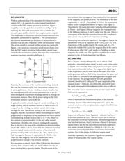
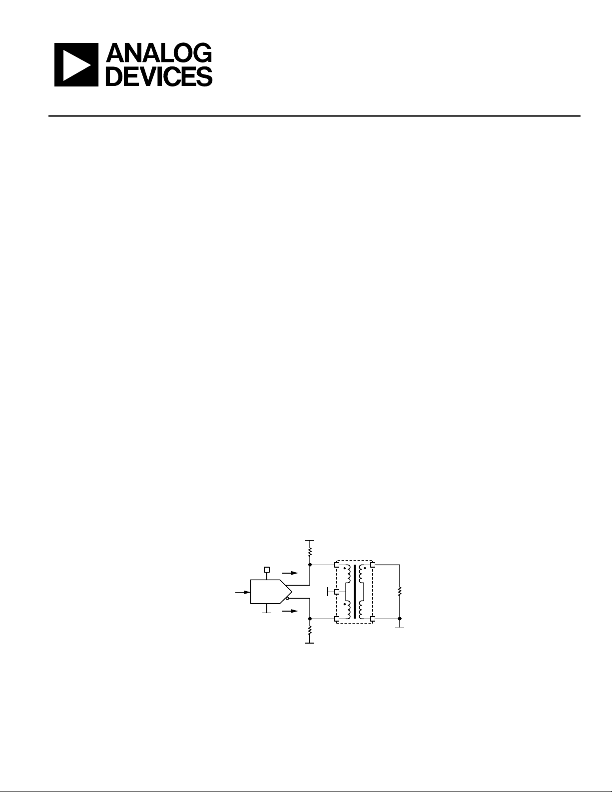
BALANCED CURRENT-OUTPUT DAC
Balanced current-output DACs come in two varieties: those
with current source outputs and those with current sink
outputs. DACs with current source outputs always inject
current into the external load, while DACs with current sink
outputs always draw current from the external load. In both
cases, the DAC output consists of two pins: a normal pin and a
complementary pin. The arrows that indicate direction of
current flow in the diagrams that follow assume conventional
current flow (that is, current flows from a positive potential
toward a negative potential).
Note that Figure 1 assumes that the DAC is of the current
sourcing variety. In the case of a current sinking DAC, the
direction of I
A
and I
B
is reversed. Also, a connection to V
SUPPLY
should replace the ground connections at the transformer
center tap and the R
O
resistors.
In this application note, the current flowing through the normal
and complementary pins is referred to as I
A
and I
B
, respectively.
The maximum current that the DAC can deliver is denoted as
I
MAX
and represents the upper limit for both I
A
and I
B
. The exact
value of I
A
(or I
B
) depends on the digital code present at the
DAC input. The behavior of I
A
and I
B
is such that when the
digital code is zero, then I
A
= 0 and I
B
= I
MAX
. Conversely, when
the digital code is full scale, then I
A
= I
MAX
and I
B
= 0. For
intermediate digital codes, the two output currents are between
zero and I
MAX
, but are balanced such that I
A
+ I
B
= I
MAX
at all
times. Thus, I
A
and I
B
can be expressed as
MAXA
II α= (1)
( )
MAX
B
II α−= 1
where α is the fractional digital code value, that is, the input
digital code value to the DAC divided by the full-scale code value.
For example, given a 10-bit DAC with an input code of 200 and
an I
MAX
value of 10 mA, then α = 200/1023 (where 1023 is the
full-scale code value given by 2
10
− 1). This yields I
A
≈ 1.955 mA
and I
B
≈ 8.045 mA. Also, notice that I
B
can be expressed in
terms of I
A
as I
B
= I
MAX
− I
A
.
1:N
R
O
R
O
R
L
V
SUPPLY
DAC
I
A
I
B
DIGITAL
CODE
0
6
7
3
7
-
0
0
1
Figure 1. A Balanced Current-Output DAC with Transformer Coupling