
herunterladen
FEATURES AND BENEFITS
• No external sense resistor required; single package solution
• Reduced power loss:
□ 0.6 mΩ internal conductor resistance on EX package
□ 1.2 mΩ internal conductor resistance on LC package
• Economical low- and high-side current sensing
• Output voltage proportional to AC or DC currents
• ±12.5 A and ±25 A full-scale sensing ranges on LC package
• ±15.5 A and ±31 A full-scale sensing ranges on EX package
• Overcurrent
¯
F
¯
¯
A
¯
¯
U
¯
¯
L
¯
¯
T
¯
trips and
latches at 100% of full-scale
current
• Low-noise analog signal path
• 100 kHz bandwidth
• Small footprint, low-profile SOIC8 and QFN packages
• 3 to 5.5 V single supply operation
• Integrated electrostatic shield for output stability
• Factory-trimmed for accuracy
• Extremely stable output offset voltage
• Zero magnetic hysteresis
• Ratiometric output from supply voltage
DESCRIPTION
The Allegro
™
ACS711 provides economical and precise
solutions for AC or DC current sensing in <100 V audio,
communications systems, and white goods. The device package
allows for easy implementation by the customer. Typical
applications include circuit protection, current monitoring,
and motor and inverter control.
The device consists of a linear Hall sensor circuit with a copper
conduction path located near the surface of the die. Applied
current flowing through this copper conduction path generates
a magnetic field which is sensed by the integrated Hall IC
and converted into a proportional voltage. Device accuracy is
optimized through the close proximity of the magnetic signal
to the Hall transducer.
The output of the device has a positive slope proportional to
the current flow from IP+ to IP– (pins 1 and 2, to pins 3 and
4). The internal resistance of this conductive path is 0.6 mΩ
for the EX package, and 1.2 mΩ for the LC package, providing
a non-intrusive measurement interface that saves power in
applications that require energy efficiency.
The ACS711 is optimized for low-side current sensing
applications, although the terminals of the conductive path
are electrically isolated from the sensor IC leads, providing
sufficient internal creepage and clearance dimensions for a
low AC or DC working voltage applications. The thickness
of the copper conductor allows survival of the device at up to
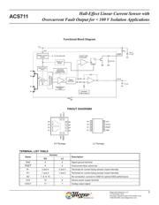
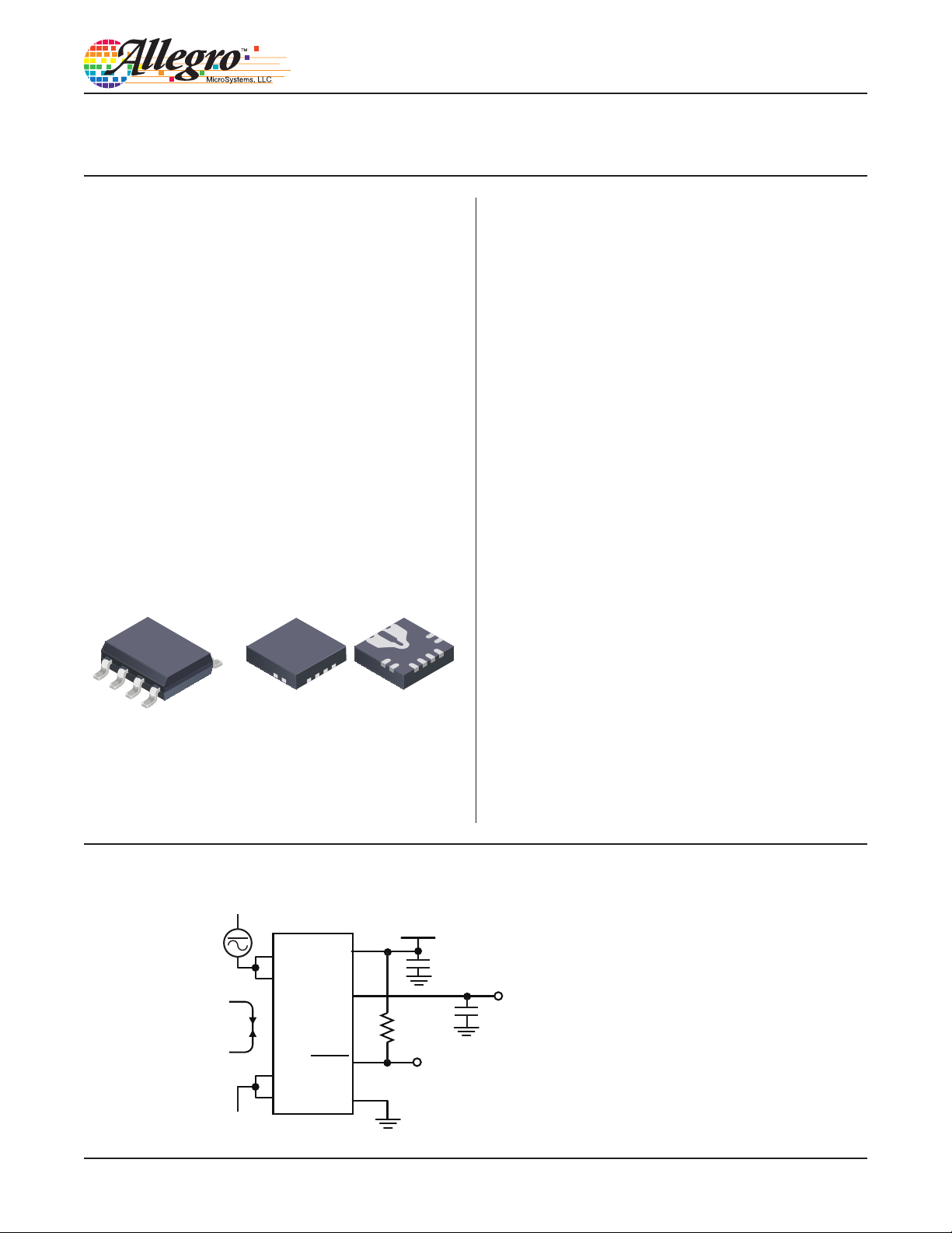
IP+
IP+
IP–
IP–
I
P
GND
ACS711
+3.3 V
VIOUT
VCC
C
BYP
0.1 μF
C
LOAD
R
PU
FAULT
ACS711
ACS711A-DS, Rev. 4
Hall-Effect Linear Current Sensor with
Overcurrent Fault Output for <100 V Isolation Applications
Continued on the next page…
Not to scale
PACKAGES:
Typical Application
8-pin SOICN
with internally fused path
(LC package)
Application 1. The ACS711 outputs
an analog signal, V
IOUT
, that varies
linearly with the bi-directional AC or
DC primary current, I
P
, within the
range specified. The
¯
F
¯
¯
A
¯
U
¯¯
L
¯
¯
T
¯
pin trips
when I
P
reaches ±100% of its full-
scale current.
12-contact QFN
3 mm × 3 mm × 0.75 mm
(EX package)
June 23, 2017
Verzeichnis