
herunterladen
1. General description
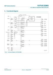
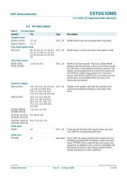
The SSTUG32865 is a 1.8 V 28-bit 1 : 2 register specifically designed for use on two rank
by four (2R × 4) and similar high-density Double Data Rate 2 (DDR2) memory modules. It
is similar in function to the JEDEC-standard 14-bit DDR2 register, but integrates the
functionality of the normally required two registers in a single package, thereby freeing up
board real-estate and facilitating routing to accommodate high-density Dual In-line
Memory Module (DIMM) designs.
The SSTUG32865 also integrates a parity function, which accepts a parity bit from the
memory controller, compares it with the data received on the D-inputs and indicates
whether a parity error has occurred on its open-drain PTYERR pin (active LOW).
It further offers added features over the JEDEC standard register in that it can be
configured for normal or high output drive strength, simply by tying input pin SELDR either
HIGH of LOW as needed. This allows use in different module designs varying from low to
high density designs by picking the appropriate drive strength to match net loading
conditions. Furthermore, the SSTUG32865 features two additional chip select inputs,
which allow more versatile enabling and disabling in densely populated memory modules.
Both added features (drive strength and chip selects) are fully backward compatible to the
JEDEC standard register.
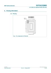
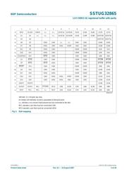
The SSTUG32865 is packaged in a 160-ball, 12 × 18 grid, 0.65 mm ball pitch, thin profile
fine-pitch ball grid array (TFBGA) package, which, while requiring a minimum
9mm× 13 mm of board space, allows for adequate signal routing and escape using
conventional card technology.
2. Features
n 28-bit data register supporting DDR2
n Fully compliant to JEDEC standard for SSTUB32865
n Supports 2 rank by 4 DIMM density by integrating equivalent functionality of two
JEDEC-standard DDR2 registers (that is, 2 × SSTUB32864 or 2 × SSTUB32866)
n Parity checking function across 22 input data bits
n Parity out signal
n Controlled multi-impedance output impedance drivers enable optimal signal integrity
and speed
n Exceeds SSTUB32865 JEDEC standard speed performance
n Supports up to 550 MHz clock frequency of operation
n Programmable for normal or high output drive
n Optimized pinout for high-density DDR2 module design
SSTUG32865
1.8 V 28-bit 1 : 2 registered buffer with parity for DDR2-1G
RDIMM applications
Rev. 01 — 16 August 2007 Product data sheet
Verzeichnis
- ・ Konfiguration des Pinbelegungsdiagramms on Seite 4 Seite 6 Seite 7
- ・ Abmessungen des Paketumrisses on Seite 23
- ・ Teilenummerierungssystem on Seite 2
- ・ Typisches Anwendungsschaltbild on Seite 3
- ・ Schweißen Temperatur on Seite 24
- ・ Beschreibung der Funktionen on Seite 1 Seite 8 Seite 14
- ・ Technische Daten on Seite 27
- ・ Anwendungsbereich on Seite 2 Seite 27