
herunterladen
© Semiconductor Components Industries, LLC, 2013
December, 2013 − Rev. 14
1 Publication Order Number:
2N4921/D
2N4921G, 2N4922G,
2N4923G
Medium-Power Plastic
NPN Silicon Transistors
These high−performance plastic devices are designed for driver
circuits, switching, and amplifier applications.
Features
• Low Saturation Voltage
• Excellent Power Dissipation Due to Thermopadt Construction
• Excellent Safe Operating Area
• Complement to PNP 2N4920G
• These Devices are Pb−Free and are RoHS Compliant**
MAXIMUM RATINGS
Rating Symbol Value Unit
Collector−Emitter Voltage
2N4921G
2N4922G
2N4923G
V
CEO
40
60
80
Vdc
Collector−Emitter Voltage
2N4921G
2N4922G
2N4923G
V
CB
40
60
80
Vdc
Emitter Base Voltage V
EB
5.0 Vdc
Collector Current − Continuous (Note 1) I
C
1.0 Adc
Collector Current − Peak (Note 1) I
CM
3.0 Adc
Base Current − Continuous I
B
1.0 Adc
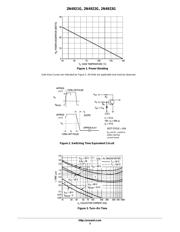
Total Power Dissipation
@ T
C
= 25_C
Derate above 25_C
P
D
30
0.24
W
mW/_C
Operating and Storage Junction
Temperature Range
T
J
, T
stg
–65 to +150
_C
Stresses exceeding those listed in the Maximum Ratings table may damage the
device. If any of these limits are exceeded, device functionality should not be
assumed, damage may occur and reliability may be affected.
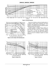
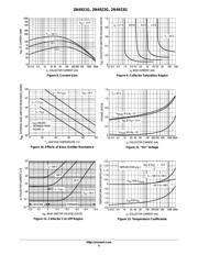
1. The 1.0 A maximum I
C
value is based upon JEDEC current gain requirements.
The 3.0 A maximum value is based upon actual current handling capability of
the device (see Figures 5 and 6).
THERMAL CHARACTERISTICS (Note 2)
Characteristic
Symbol Max Unit
Thermal Resistance, Junction−to−Case
R
q
JC
4.16
_C/W
2. Recommend use of thermal compound for lowest thermal resistance.
*Indicates JEDEC Registered Data.
** For additional information on our Pb−Free strategy and soldering details,
please download the ON Semiconductor Soldering and Mounting Techniques
Reference Manual, SOLDERRM/D.
1.0 AMPERE
GENERAL PURPOSE
POWER TRANSISTORS
40−80 VOLTS, 30 WATTS
http://onsemi.com
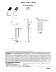
MARKING DIAGRAM
Y = Year
WW = Work Week
2N492x = Device Code
x = 1, 2, or 3
G = Pb−Free Package
Device Package Shipping
ORDERING INFORMATION
2N4921G TO−225
(Pb−Free)
500 Units / Box
2N4922G TO−225
(Pb−Free)
500 Units / Box
2N4923G TO−225
(Pb−Free)
500 Units / Box
3
BASE
1
EMITTER
COLLECTOR
2, 4
TO−225
CASE 77−09
STYLE 1
1
2
3
YWW
2
N492xG
Verzeichnis